Key Takeaways
- Definition: An LDMOS PA PCB is a specialized circuit board designed to support Laterally Diffused Metal Oxide Semiconductor transistors, primarily used in high-power RF amplification for base stations and radar.
- Thermal Criticality: Unlike standard logic boards, the primary failure mode for LDMOS applications is thermal runaway; effective heat dissipation strategies (copper coins, via farms) are non-negotiable.
- Material Hierarchy: While FR4 is cheap, LDMOS designs almost exclusively require high-frequency laminates (like Rogers or Taconic) or hybrid stackups to maintain signal integrity.
- Grounding: Source grounding is critical for RF performance; the PCB manufacturing process must ensure ultra-low inductance paths to the ground plane.
- Validation: Standard electrical testing is insufficient; passive intermodulation (PIM) testing and thermal cycling are required to validate the bond between the LDMOS flange and the PCB.
- LSI Context: While GaN PA PCB and GaAs PA PCB technologies are gaining ground for higher frequencies, LDMOS remains the dominant, cost-effective choice for high-power applications below 4 GHz.
- Manufacturing Precision: The tolerance for track width etching in LDMOS designs is often tighter than +/- 0.5 mil due to impedance matching requirements.
What LDMOS Power Amplifier (PA) PCB really means (scope & boundaries)
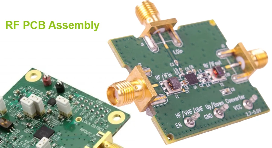
Building on the core definition, understanding an LDMOS PA PCB requires looking beyond the component itself and viewing the board as an integral part of the thermal and electrical system. LDMOS (Laterally Diffused Metal Oxide Semiconductor) technology has been the workhorse of the RF power industry for decades, particularly in cellular infrastructure (4G/LTE and sub-6GHz 5G), broadcast transmitters, and L-band radar systems.
When we discuss the PCB for these amplifiers, we are not talking about a simple carrier board. The PCB acts as the primary heat sink interface and the critical matching network for the RF signal. LDMOS devices typically operate with drain efficiencies between 50% and 70%. This means that for a 100W output signal, the device might generate 40W to 100W of waste heat. If the PCB cannot transfer this heat away from the transistor flange immediately, the junction temperature will rise, linearity will degrade, and the device will eventually fail.
Furthermore, the "PA" (Power Amplifier) aspect dictates that the board must handle high currents and high voltages simultaneously. The dielectric breakdown voltage of the material becomes a safety factor. Unlike low-power GaAs PA PCB designs used in mobile handsets, or high-frequency GaN PA PCB designs used in satellite communications, LDMOS boards occupy a specific niche: high power, medium frequency (HF to ~3.5 GHz), and high linearity requirements.
At APTPCB (APTPCB PCB Factory), we see that the manufacturing complexity lies in the hybrid nature of these boards. Designers often combine high-frequency laminates (for the RF signal path) with standard FR4 (for control logic and DC bias lines) to manage costs. This creates a "hybrid stackup" that presents unique challenges during lamination due to different thermal expansion rates of the materials.
LDMOS Power Amplifier (PA) PCB metrics that matter (how to evaluate quality)
To ensure the board can handle the rigorous demands of high-power RF signals, we must move from general definitions to quantifiable metrics. The following table outlines the specific physical and electrical properties that define the quality of an LDMOS PA PCB.
| Metric | Why it matters | Typical range or influencing factors | How to measure |
|---|---|---|---|
| Thermal Conductivity (k) | Determines how fast heat moves from the LDMOS flange through the PCB to the heatsink. Low 'k' leads to hotspots. | 0.5 W/mK (FR4) to 390 W/mK (Copper). High-performance dielectrics range from 0.6 to 1.3 W/mK. | Laser Flash Analysis (LFA) or steady-state heat flow meter. |
| Dielectric Constant (Dk) | Dictates the width of transmission lines for a specific impedance. Stability of Dk over frequency is crucial for matching networks. | 2.2 to 10.2. Common RF materials are 3.0 to 3.66. Tighter tolerance (+/- 0.05) is better. | Split Post Dielectric Resonator (SPDR) method. |
| Dissipation Factor (Df) | Represents signal loss as heat within the dielectric. High Df kills efficiency in high-power PAs. | 0.001 to 0.004 for RF materials. Standard FR4 is 0.020 (too high for RF path). | Cavity perturbation method. |
| Coefficient of Thermal Expansion (CTE-z) | If the PCB expands faster than the copper via barrel during heating, the vias will crack (open circuit). | 20-70 ppm/°C. Lower is better for reliability, especially in thick boards. | Thermomechanical Analysis (TMA). |
| Peel Strength | High power generates heat, which can delaminate copper traces. LDMOS leads exert physical stress. | > 0.8 N/mm (standard), but > 1.4 N/mm is preferred for high-reliability PA boards. | 90-degree peel test. |
| Surface Roughness | At RF frequencies, current flows on the "skin" of the copper. Rough copper increases resistance and loss. | 0.5 µm to 2.0 µm. "Reverse treated" or "Very Low Profile" (VLP) copper is preferred. | Profilometer or SEM cross-section. |
| Glass Transition Temp (Tg) | The temperature where the PCB resin turns soft. LDMOS boards run hot, requiring high Tg to prevent mechanical failure. | > 170°C (High Tg) is standard for PA applications. | DSC (Differential Scanning Calorimetry). |
How to choose LDMOS Power Amplifier (PA) PCB: selection guidance by scenario (trade-offs)
Understanding the metrics allows engineers to select the right PCB architecture, but the "best" choice depends entirely on the specific application scenario. Here are six common scenarios for LDMOS PA PCB implementation and the recommended trade-offs for each.
Scenario 1: High-Power Base Station (Macro Cell)
- Requirement: Continuous high power (100W+), 24/7 operation, 10-year lifespan.
- Recommendation: Embedded Copper Coin PCB.
- Trade-off: This is the most expensive manufacturing option. It involves embedding a solid copper slug directly into the PCB under the LDMOS component.
- Why: Thermal vias are insufficient for this power density. The copper coin provides a direct thermal path to the chassis.
- Risk: If the coin is not perfectly planar with the PCB surface, soldering the LDMOS component will fail (voids).
Scenario 2: Cost-Sensitive Broadcast Transmitter
- Requirement: Medium power, lower frequency (FM/VHF), tight budget.
- Recommendation: Hybrid Stackup (FR4 + Rogers) with Thermal Vias.
- Trade-off: More complex lamination process than pure FR4, but cheaper than a full RF material board.
- Why: You only use expensive RF material on the top layer where the signal travels. The bottom layers (power/control) use cheap FR4.
- Risk: Warpage. The CTE mismatch between FR4 and Rogers can cause the board to bow during reflow if the stackup is not balanced.
Scenario 3: High-Frequency Radar (S-Band)
- Requirement: Pulse signals, precise impedance control, low loss.
- Recommendation: Ceramic-filled PTFE (e.g., Rogers RO3000 series).
- Trade-off: Material is soft and difficult to machine. Dimensional stability is tricky.
- Why: PTFE offers the lowest possible loss (Df) and stable Dk.
- Risk: "Smear" during drilling. The soft material can smear over copper connections if drill speeds are not optimized.
- Internal Link: See our capabilities in High Frequency PCB Manufacturing for more details on PTFE handling.
Scenario 4: Prototype / Proof of Concept
- Requirement: Fast turnaround, validating electrical design only.
- Recommendation: Standard Rogers 4350B (Double Sided).
- Trade-off: No complex multilayer features. Limited thermal management (just vias).
- Why: 4350B processes like FR4, making it fast and cheap to fabricate for quick tests.
- Risk: Cannot run at full power for long periods without an external heatsink clamp.
Scenario 5: Space-Constrained Small Cell
- Requirement: High density, active antenna systems (AAS).
- Recommendation: HDI (High Density Interconnect) with Blind/Buried Vias.
- Trade-off: High manufacturing cost and complexity.
- Why: You need to route complex bias and control lines in a small footprint while keeping the RF path clean.
- Risk: Signal crosstalk. With lines closer together, isolation between the PA output and input becomes critical to prevent oscillation.
Scenario 6: Legacy Replacement (2G/3G Maintenance)
- Requirement: Matching obsolete specs, drop-in replacement.
- Recommendation: Reverse Engineering / Material Substitution.
- Trade-off: Original materials may be discontinued.
- Why: Modern materials often have different Dk values than materials from 20 years ago. You may need to adjust trace widths to match the original impedance.
- Risk: Performance drift. The new board might be "too good" (less loss), changing the gain profile of the amplifier.
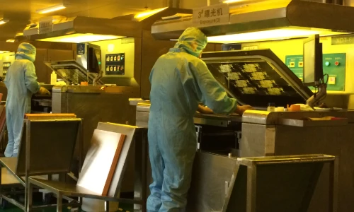
LDMOS Power Amplifier (PA) PCB implementation checkpoints (design to manufacturing)

Once the architecture is selected, the transition from a CAD file to a physical board is where most failures occur. This section outlines the critical checkpoints in the manufacturing process for an LDMOS PA PCB.
1. Material Sourcing and Storage
- Checkpoint: Verify the specific laminate batch.
- Recommendation: For high-end PA applications, request "Dk-sorted" materials where the manufacturer guarantees the dielectric constant is within a tighter tolerance than standard.
- Risk: RF materials are hygroscopic (absorb moisture). If not stored in vacuum packs, they will delaminate during reflow.
- Acceptance: Moisture content test before lamination.
2. Inner Layer Imaging and Etching
- Checkpoint: Trace width precision.
- Recommendation: Use Laser Direct Imaging (LDI) rather than traditional film. LDMOS matching networks rely on precise line widths/lengths for impedance transformation.
- Risk: Over-etching increases impedance; under-etching decreases it. A 1-mil error can shift the frequency response by MHz.
- Acceptance: Automated Optical Inspection (AOI) with strict tolerance settings (+/- 10%).
3. Hybrid Lamination (Bonding)
- Checkpoint: Bonding different materials (e.g., PTFE to FR4).
- Recommendation: Use specific "bond ply" or prepreg designed for dissimilar materials. The press cycle (temperature ramp-up and cool-down) must be customized to minimize stress.
- Risk: Delamination or registration errors (layers shifting) due to different expansion rates.
- Acceptance: Microsection analysis to check bond line integrity.
- Internal Link: Learn more about complex layups in our PCB Stack-up guide.
4. Drilling and Via Formation
- Checkpoint: Grounding vias near the LDMOS source.
- Recommendation: Use a "via farm" (dense array of vias) directly under the component ground pad.
- Risk: If the drill bit is dull, it creates rough hole walls, leading to poor plating and high inductance.
- Acceptance: Cross-section verification of hole wall quality.
5. Copper Coin Insertion (If applicable)
- Checkpoint: Press-fit or bonded coin integration.
- Recommendation: The coin must be plated over to ensure a solderable surface. The transition from PCB surface to coin surface must be less than 50 microns (flatness).
- Risk: If the coin sits too high, the component rocks; if too low, solder voids form.
- Acceptance: 3D profilometry scanning of the surface flatness.
6. Plating (Surface Finish)
- Checkpoint: Conductivity and oxidation protection.
- Recommendation: Immersion Silver or ENIG (Electroless Nickel Immersion Gold). Silver is preferred for RF because it has no nickel (nickel is ferromagnetic and can cause passive intermodulation/PIM).
- Risk: HASL (Hot Air Solder Leveling) is too uneven for LDMOS components.
- Acceptance: X-ray fluorescence (XRF) to measure plating thickness.
7. Solder Mask Application
- Checkpoint: Covering non-critical areas.
- Recommendation: Keep solder mask off the RF transmission lines if possible. Solder mask adds a layer of dielectric that is lossy and hard to control.
- Risk: Applying mask over RF lines changes the impedance (usually drops it by 2-3 ohms) and increases loss.
- Acceptance: Visual inspection against Gerber "keep-out" layers.
8. Routing and Profiling
- Checkpoint: Edge quality.
- Recommendation: The board edges should be smooth and free of copper burrs.
- Risk: Copper burrs at the edge can cause arcing in high-power/high-voltage applications.
- Acceptance: Visual inspection.
9. Electrical and Thermal Testing
- Checkpoint: Final validation.
- Recommendation: Beyond open/short testing, perform TDR (Time Domain Reflectometry) for impedance and Hi-Pot testing for dielectric breakdown.
- Risk: A board that passes continuity might still fail at 2GHz due to impedance mismatches.
- Acceptance: TDR report and Certificate of Compliance (CoC).
LDMOS Power Amplifier (PA) PCB common mistakes (and the correct approach)
Even with a robust process, specific errors frequently plague LDMOS PA PCB projects. Identifying these early can save weeks of revision time.
Ignoring the "Skin Effect" on Surface Finish:
- Mistake: Using ENIG for very high-power, high-frequency LDMOS designs.
- Correction: While ENIG is flat and reliable, the Nickel layer is magnetic and has higher resistance. At RF frequencies, current travels in this Nickel layer, increasing loss. Use Immersion Silver or ENEPIG (if designed correctly) for sensitive PAs.
Inadequate Grounding of the Source:
- Mistake: Connecting the LDMOS source pad to ground using only a few thermal vias.
- Correction: The source inductance must be minimized to maintain gain. Use the maximum number of vias possible (via farm) or a copper coin. The inductance of a via is non-trivial at GHz frequencies.
Overlooking CTE Mismatch in Hybrid Boards:
- Mistake: Designing a stackup with Rogers on top and FR4 on the bottom without balancing copper density.
- Correction: Ensure the stackup is symmetrical in terms of copper weight and dielectric thickness where possible to prevent the "potato chip" warping effect during reflow.
Placing Solder Mask on the RF Path:
- Mistake: Fully covering the RF input/output traces with solder mask for protection.
- Correction: Use "solder mask defined" pads only where necessary. Leave the RF traces bare (or plated) or account for the mask's Dk in the simulation. The mask adds unpredictable capacitance.
Neglecting Thermal Via Plugging:
- Mistake: Leaving thermal vias under the component open (unplugged).
- Correction: Solder will wick down open vias during reflow, leaving the LDMOS flange "starved" of solder. This creates voids and leads to thermal failure. Always use capped or filled and plated vias (VIPPO) for pads under components.
- Internal Link: Review our guidelines on DFM Guidelines to understand via plugging options.
Incorrect Copper Weight Specification:
- Mistake: Using standard 1oz copper for high-current drain lines.
- Correction: Calculate the current density. LDMOS drains can pull significant amps. Use 2oz or 3oz copper for DC feed lines to minimize voltage drop and resistive heating.
LDMOS Power Amplifier (PA) PCB FAQ (cost, lead time, Design for Manufacturability (DFM) files, stackup, impedance, Dielectric Constant (DK)/Dissipation Factor (DF))
Q: Can I use GaN on an LDMOS PA PCB design? A: Generally, no. GaN PA PCB designs typically require different bias voltages (negative gate voltage) and often operate at higher impedances and frequencies. While the footprint might look similar, the thermal and electrical matching networks are different.
Q: Why is Immersion Silver preferred over ENIG for LDMOS? A: Immersion Silver has higher conductivity and lacks the magnetic nickel layer found in ENIG. This results in lower insertion loss and better PIM (Passive Intermodulation) performance, which is critical for modern cellular base stations.
Q: What is the difference between a "Copper Coin" and "Heavy Copper"? A: Heavy copper refers to the thickness of the foil on the layer (e.g., 3oz or 4oz). A copper coin is a solid slug of copper (several millimeters thick) embedded into the board. Coins offer superior vertical thermal transfer compared to heavy copper layers.
Q: How do I specify the "weave" of the glass fiber? A: For high-frequency LDMOS boards, the glass weave effect can cause signal skew. You should specify "spread glass" (e.g., 1067 or 1078 style) rather than open weaves (like 106 or 7628) to ensure a consistent Dk across the trace.
Q: What is the shelf life of an LDMOS PCB with Immersion Silver? A: Immersion Silver is sensitive to tarnishing (sulfur). The shelf life is typically 6 to 12 months if kept in sealed vacuum bags with desiccant and humidity indicator cards. Once opened, it should be soldered within 24 hours.
Q: Do I need back-drilling for LDMOS boards? A: If your design uses through-hole vias for signal transitions (less common in PA, but possible), back-drilling is essential to remove the "stub" which acts as an antenna and causes signal reflection.
Q: Why does APTPCB recommend "dummy copper" on hybrid boards? A: Dummy copper (thieving) helps balance the copper distribution on the layers. This ensures even pressure during lamination and even plating thickness, reducing the risk of bow and twist in hybrid builds.
Q: Is "sweat soldering" necessary for LDMOS? A: Yes. The large metal flange on the bottom of the LDMOS package must be soldered to the PCB ground/heatsink pad. This process, often called sweat soldering or reflow of the flange, is the primary thermal path. Voids here are catastrophic.
Resources for LDMOS Power Amplifier (PA) PCB (related pages and tools)
To assist in your design process, APTPCB provides several tools and resources that directly relate to LDMOS and RF PCB design:
- Impedance Calculator: Verify your trace widths against your stackup before submitting files.
- Material Library: Compare the Dk and Df of Rogers, Isola, and Panasonic materials.
- Gerber Viewer: Check your files for errors like solder mask on RF lines.
- DFM Check: Submit your design for a manufacturability review to catch thermal via issues early.
LDMOS Power Amplifier (PA) PCB glossary (key terms)
| Term | Definition |
|---|---|
| P1dB | The output power level where the amplifier gain drops by 1dB from its linear response. A key metric for PA linearity. |
| IP3 (Third-Order Intercept) | A measure of the linearity of the amplifier. Higher IP3 means less distortion (intermodulation) between signals. |
| VSWR (Voltage Standing Wave Ratio) | A measure of how efficiently RF power is transmitted. High VSWR means power is reflecting back to the source (bad matching). |
| CTE (Coefficient of Thermal Expansion) | The rate at which a material expands when heated. Mismatch between copper and dielectric causes failure. |
| Tg (Glass Transition Temperature) | The temperature at which the PCB substrate transitions from a hard, glassy state to a soft, rubbery state. |
| Dk (Dielectric Constant) | The ratio of the permittivity of a substance to the permittivity of free space. Affects signal speed and impedance. |
| Df (Dissipation Factor) | A measure of the power loss rate of the electrical energy in a dielectric material (signal loss). |
| Skin Effect | The tendency of high-frequency alternating current to distribute itself within the conductive material so that the current density is largest near the surface. |
| PIM (Passive Intermodulation) | Unwanted signals generated by the non-linear mixing of 2 or more frequencies in passive devices (like connectors or PCB traces). |
| Via Farm | A dense cluster of vias used to conduct heat or current between layers, typically placed under a hot component. |
| VIPPO (Via-in-Pad Plated Over) | A technology where vias are placed in the component pad, filled with epoxy, and plated over to create a flat surface. |
| Hybrid Stackup | A PCB layup that combines two different types of laminate materials (e.g., FR4 and Rogers) to balance cost and performance. |
Conclusion (next steps)
Designing and manufacturing an LDMOS PA PCB is an exercise in balancing thermal thermodynamics with RF physics. It requires a shift in mindset from "connecting pins" to "managing fields and heat." Whether you are building a massive base station amplifier or a specialized radar module, the success of the project hinges on the integrity of the PCB substrate, the precision of the etching, and the robustness of the thermal management strategy.
At APTPCB, we specialize in these high-reliability, high-power RF boards. We understand that a void in the solder joint or a variation in the dielectric constant can mean the difference between a functioning transmitter and a failed system.
Ready to move to production? When submitting your data for a quote or DFM review, please ensure you provide:
- Gerber Files (RS-274X format).
- Stackup Drawing specifying the exact material (e.g., Rogers 4350B 20mil).
- Drill Chart indicating plated vs. non-plated holes.
- Surface Finish Requirement (e.g., Immersion Silver).
- Impedance Requirements (e.g., 50 ohm traces on Layer 1).
- Special Requirements (e.g., Copper coin, countersink, or specific via plugging).
Contact our engineering team today to ensure your LDMOS designs are built to perform.