
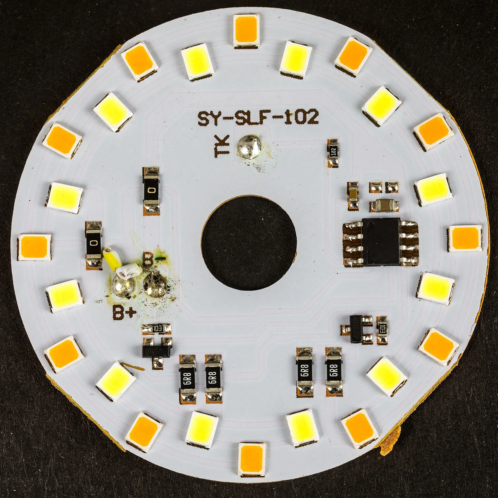
- An LED MCPCB should be reviewed as a high-thermal-mass assembly, not as an FR4 board that happens to have metal on the back.
- The first assembly question is whether heat moves predictably through the dielectric layer during reflow, because that same layer is both the working heat path and the most stressed interface.
- A board can pass placement and look correct under AOI while the real problem is an uneven heat-up that left cold joints, tombstoned parts, or voids hiding under the LED thermal pad.
- A reflow profile tuned on FR4 usually transfers poorly to a metal core, so the profile, not the layout, is often where a metal-core build first goes wrong.
- Keep the review at the board and process boundary. It does not predict in-service lumen output, LED lifetime, or finished-luminaire thermal performance.
Quick Answer An
LED MCPCBis best reviewed as a board whose metal core soaks up heat far faster than fiberglass, sitting under a thin dielectric that has to carry that heat without being stressed into damage. The practical pre-build question is notDoes the layout look right?It isDoes the reflow profile actually bring the metal core to soldering temperature evenly, and can X-ray confirm the thermal path under the LED is real before volume build?
Table of Contents
- What an LED MCPCB is — and what it is not
- The physical boundary: heat path through the dielectric
- What changes in reflow on a metal-core board
- Release implications: what to confirm before volume build
- FAQ
- Public references
- Author and review information
What an LED MCPCB is — and what it is not
An LED metal-core PCB (MCPCB), sometimes called an insulated metal substrate (IMS), is built around a base metal plate, most often aluminum, sometimes copper. On top of that plate sits a thin dielectric layer, and on top of that the copper circuit that carries the LEDs. That stack is the whole point of the construction: heat from the LED is meant to drop almost straight down through the copper, through the dielectric, and into the metal plate, which spreads and holds it.
It is useful to be clear about what an MCPCB is not. It is not an FR4 board with better thermals. On a standard FR4 board, heat from a hot part has to travel laterally through copper or down through thermal vias, and the fiberglass laminate itself is a poor conductor. On an MCPCB the dielectric is engineered to move heat vertically while still isolating the circuit electrically from the metal base. That single layer is doing two jobs at once, and they pull against each other: a thinner dielectric moves heat better but offers less voltage isolation, while a thicker one isolates better but adds thermal resistance. Where that trade-off lands is a selection decision tied to the laminate datasheet and the operating voltage, not a universal "best" value.
An MCPCB is also usually not a high-layer-count routing solution. The construction is most natural as a single conductive layer over the dielectric and plate, so a design that needs dense multi-layer signal routing is often a different problem than a thermal one. For the substrate selection itself, the primary reference is Metal Core PCB. When the driving constraint is moving heat out rather than the metal backing specifically, High Thermal PCB frames the wider set of options, and Heavy Copper PCB is worth comparing where lateral spreading in thick copper is part of the strategy.
The reason the distinction matters for assembly is simple: the thing that makes an MCPCB good in service — a metal mass that absorbs and holds heat — is exactly the thing that makes it behave differently in the reflow oven. You cannot treat the board as electrically equivalent to FR4 and assume the same process carries over.
The physical boundary: heat path through the dielectric
The dielectric layer is the center of gravity for both performance and risk. In service, it is the bottleneck of the heat path: the LED die can be excellent and the metal plate can be highly conductive, but the system is limited by how well the dielectric passes heat from copper to core. In assembly, that same layer sits between two materials that expand at different rates when heated, so it is also where thermal-mechanical stress concentrates.
A few boundary-level points are worth holding onto without attaching invented numbers to them:
- The dielectric is a thermal series element. Its conductivity and thickness, as stated on the laminate datasheet, set how much thermal resistance sits between the LED and the core. Treat those as inputs to confirm, not as targets to assert.
- The dielectric is also the isolation barrier. Whatever isolation the board needs to survive — confirmed by the laminate spec and any hi-pot requirement — depends on this layer staying intact through fabrication, routing, and assembly handling.
- The metal core and the copper and the dielectric all have different coefficients of thermal expansion. Heating and cooling the stack moves these layers against each other. The dielectric is the thin interface caught in the middle.
This is why the heat path is not just a layout question. A void under the LED thermal pad, a micro-crack in the dielectric from rough depaneling, or a region where solder never fully wetted all interrupt that vertical path. The board can still light up and still pass continuity, because none of those defects is an open circuit. They are thermal defects, and they are mostly invisible to electrical test and to a top-down optical look. For where this fits in the broader construction picture, PCB Stack-Up gives the layer-definition context, and surface-finish choices that affect wetting flatness are covered in PCB Surface Finishes.
What changes in reflow on a metal-core board
The single biggest change is thermal mass. The metal core stores a great deal of heat and comes up to temperature more slowly than the air around it. A profile that was developed on FR4, where the laminate heats fairly close to the air temperature, transfers poorly here: the oven air may reach the intended zone while the actual board surface lags well behind. The fix is not a single number but a profile reasoning. The soak portion of the cycle generally has to give the core more time to reach equilibrium before peak, and the only reliable way to know what the board is actually doing is to attach thermocouples to the board surface rather than trusting the air probe. Exact soak times, ramp rates, and peak temperatures belong to your assembly profile and the solder paste and LED datasheets, not to a universal recommendation.
The risk chain on a metal-core board flows directly out of that thermal mass. It runs like this:
- The high thermal mass and the thin dielectric mean the board does not heat up uniformly; a thermal gradient develops across the assembly during reflow.
- That uneven heat-up produces uneven solder melting. One pad of a small LED can reach liquidus before the other, and the surface-tension imbalance pulls the part upright — tombstoning — or skews it off its pads.
- Under larger LED thermal pads, flux volatiles that cannot escape get trapped as the solder solidifies, leaving voids; meanwhile the CTE mismatch across the heating-and-cooling cycle loads the dielectric.
- The result is degraded thermal contact under the part — a void or a partially wetted joint is an air gap in the one path that was supposed to carry heat down — and that lost contact is what shows up later as thermal and lumen performance loss once the board is actually running.
The important thing about this chain is that its early stages are quiet. A tombstoned part is at least visible. A void under a thermal pad, or a joint that wetted on one side only, usually is not. This is the side note that matters most for a metal-core build: the defect that hurts in-service thermal performance is often the one electrical test and top-down AOI will pass. That is why X-ray is the practical tool here — it can see voiding and coverage under the LED thermal pad that no surface inspection reaches. The point is not a void-percentage threshold, which depends on your application and acceptance criteria; the point is that without X-ray you are releasing the thermal path on faith.
Two more process realities follow from the same metal mass. Cooling is not a free zone: pulling a metal-core board down too quickly locks in stress from the CTE mismatch and can bow the board, which then will not sit flat against its heatsink. And rework is genuinely harder, because a soldering iron alone loses the fight against a core that wicks heat away; a preheated base is usually needed to bring the board up before any local work. For how these inspection and placement steps fit a normal SMT flow, see SMT and THT Assembly; for the void-detection step specifically, X-Ray Inspection; and for surface-level coverage and polarity, AOI Inspection. The stencil strategy that lets flux vent out from under a large pad is part of PCB Stencil.
Release implications: what to confirm before volume build
Use a staged confirmation before committing to volume, rather than assuming the prototype profile scales. The goal is to verify the heat path is real and the process is stable, not to prove any finished-luminaire outcome.
| Confirm before volume build | What to look for | Why it is a release issue |
|---|---|---|
| Profile was developed on the actual board, not inherited from FR4 | Thermocouples were attached to the board surface and the soak gives the core time to reach temperature before peak | The metal core lags the air; an inherited profile risks cold joints across the whole build |
| Thermal path under the LED is inspected, not assumed | X-ray coverage of the LED thermal pad, read against your own acceptance criteria | Voids and one-sided wetting pass electrical test and top-down AOI but block the working heat path |
| Stencil lets flux escape from large thermal pads | Aperture strategy provides venting channels rather than one solid full-coverage print | Trapped volatiles under a big pad are a primary voiding source on metal core |
| Dielectric integrity survived handling and depaneling | Edges, isolation expectation per the laminate datasheet, and any hi-pot requirement are confirmed | The dielectric is both heat path and isolation barrier; damage there is hard to see and serious |
| Cooling and flatness are controlled | Cooling ramp avoids locking in CTE stress; board sits flat enough to mount | A bowed metal-core board breaks contact with its heatsink no matter how good the joints are |
| Review language stays at the board boundary | Claims stay on profile, inspection, and manufacturability, not LED lifetime or luminaire thermal results | A board-and-process review should not be read as a finished-product performance guarantee |
If the package still needs stackup or manufacturing-note alignment before release, the companion resource is DFM Guidelines, and for inspection and validation language at board level the closest support page is Testing and Quality. High-power LED arrays for infrastructure and signaling often share constraints with Communication Equipment PCB builds, where thermal substrates and assembly inspection overlap.
When the design and profile reasoning are settled and you want a manufacturing review against your own files and acceptance criteria, the metal core PCB thermal review request is the place to start that conversation.
FAQ
Why does an LED MCPCB need a different reflow profile than FR4?
Because the metal core stores and absorbs heat far faster than fiberglass. A profile tuned on FR4 tends to leave the metal-core board below soldering temperature when the air reaches peak, which risks cold joints. The soak generally has to give the core time to catch up, and the actual board temperature should be confirmed with surface thermocouples rather than the air probe.
What failure shows up first on a metal-core build, and is it visible?
Tombstoning or skewed parts from uneven heat-up are at least visible. The more dangerous defect is voiding or one-sided wetting under the LED thermal pad, which interrupts the heat path but usually passes electrical test and top-down AOI. That is the defect that tends to surface later as lost thermal contact.
Why is X-ray emphasized for these boards?
The LED thermal pad sits under the part, so surface inspection cannot see whether solder actually covered it or whether voids opened up. X-ray is a non-destructive way to read coverage and voiding under the pad. Acceptance limits depend on your application and criteria, so treat X-ray as the confirmation step rather than a fixed pass number.
Is a thinner dielectric always better because it moves heat better?
No. A thinner dielectric lowers thermal resistance but also reduces voltage isolation, while a thicker one isolates better but adds thermal resistance. Where that trade-off lands depends on the operating voltage and the laminate datasheet, so it is a selection decision rather than a universal best.
Should I choose copper core instead of aluminum core?
Both are valid families. Aluminum is common, lighter, and lower cost; copper spreads heat more aggressively but is heavier and more expensive. The right choice is a trade-off against the design's thermal demand, weight, and budget, confirmed against the laminate options rather than assumed from a ranking.
Can I rework a single LED on a finished MCPCB?
It is possible but harder than on FR4. The metal core wicks heat away from a soldering iron, so a preheated base is generally needed to bring the board up to temperature before local work, and care is needed not to disturb neighboring joints or the dielectric.
Public references
Metal Core PCB Primary support page for metal-core and IMS substrate selection and construction.
High Thermal PCB Support-page context for the wider set of heat-removal substrate options.
PCB Stack-Up Support-page context for layer definition and controlled construction planning.
SMT and THT Assembly Support-page context for the assembly flow these boards pass through.
X-Ray Inspection Support-page context for non-destructive void and coverage inspection under thermal pads.
DFM Guidelines Support-page context for manufacturing review intake and pre-release clarification.
Author and review information
- Author: APTPCB editorial team
- Technical review: PCBA assembly and thermal-substrate review team
- Review scope: Board-level and process-level review of metal-core construction, reflow profiling, inspection, and pre-build release consistency