Contents
- The Context: What Makes LIDAR Security PCB Challenging
- The Core Technologies (What Actually Makes It Work)
- Ecosystem View: Related Boards / Interfaces / Manufacturing Steps
- Comparison: Common Options and What You Gain / Lose
- Reliability & Performance Pillars (Signal / Power / Thermal / Process Control)
- The Future: Where This Is Going (Materials, Integration, Ai/automation)
- Request a Quote / DFM Review for LIDAR Security PCB (What to Send)
- Conclusion
For engineers and procurement teams, a "good" LIDAR Security PCB is defined by its ability to handle high-current pulses without noise, maintain signal integrity for precise Time-of-Flight (ToF) calculations, and survive years of outdoor exposure. It is not just a carrier for components; it is an active element in the optical system's accuracy.
Highlights
- Nanosecond Timing: Trace length matching is critical for accurate distance measurement.
- Thermal Management: High-power laser diodes require specialized heat dissipation strategies.
- Material Selection: Low-loss laminates are often necessary to preserve signal fidelity.
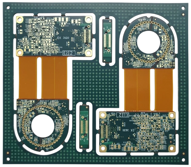
- Rigid-Flex Integration: Many LIDAR units use rotating heads or compact housings requiring flexible interconnects.
The Context: What Makes LIDAR Security PCB Challenging
The shift from passive video recording to active 3D sensing introduces a new set of engineering constraints. Unlike a standard Network Security PCB that primarily handles digital video streams, a LIDAR board is a mixed-signal powerhouse. It must manage the violent switching noise of laser drivers alongside the whisper-quiet sensitivity of photodetectors (like APDs or SPADs).
The primary challenge is the speed of light. In a Time-of-Flight system, the distance is calculated by measuring how long it takes for a laser pulse to return. Light travels approximately 30 centimeters in one nanosecond. If the PCB layout introduces even a slight impedance mismatch or signal skew, the resulting distance measurement can drift by centimeters or meters, rendering the Perimeter Security PCB ineffective for precise intrusion detection.
Furthermore, these devices are often deployed outdoors. They face direct sunlight, freezing rain, and humidity. The PCB must withstand significant thermal cycling without delamination or via cracking. This requires a careful balance between electrical performance (using high-frequency materials) and mechanical robustness (using materials with appropriate CTE values).
The Core Technologies (What Actually Makes It Work)
To achieve the necessary performance, the manufacturing of a LIDAR Security PCB relies on several advanced fabrication technologies. These are not optional "nice-to-haves" but are fundamental to the physics of LIDAR operation.
1. High-Density Interconnect (Hdi) and Microvias
Modern LIDAR sensors, especially solid-state variants, pack thousands of emitters and sensors into a small footprint. To route these signals out to the processing unit (FPGA or ASIC), HDI PCB technology is essential. Laser-drilled microvias allow for tighter component placement and shorter signal paths. Shorter paths reduce parasitic inductance and capacitance, which is vital for maintaining the sharp rise times of the laser pulses.
2. Advanced Thermal Structures
Firing lasers, even for nanoseconds, generates significant localized heat. If the laser diode heats up, its wavelength can shift, and its efficiency drops. To combat this, designers often utilize High Thermal PCB techniques. This might involve copper coin embedding, where a solid piece of copper is inserted directly under the laser component, or the use of Metal Core PCBs (MCPCB) for the emitter sub-assembly. Efficient heat extraction ensures the device remains within its safe operating area (SOA) during continuous scanning.
3. Low-Loss Material Integration
Standard FR4 materials act like a sponge to high-frequency signals, absorbing energy and distorting the pulse shape. For the high-speed analog front end, manufacturers often use hybrid stackups. This involves pressing a layer of high-frequency material (like Rogers or Taconic) together with standard FR4. The critical high-speed signals travel on the advanced material, while the less critical power and control logic reside on the cheaper FR4 layers.
Ecosystem View: Related Boards / Interfaces / Manufacturing Steps
A LIDAR sensor rarely operates in isolation. It is part of a broader security ecosystem that includes access control, video analytics, and central management.
The Interconnected Security Stack
The data generated by the LIDAR unit—a dense point cloud—is heavy. It requires high-bandwidth interfaces to transmit this data to a Security Analytics PCB located in a server room or an edge gateway. Common interfaces include Gigabit Ethernet or Automotive Ethernet (1000BASE-T1). The PCB design must strictly follow the impedance requirements for these differential pairs to prevent packet loss.
In many facilities, the LIDAR system works in tandem with a Security Badge PCB reader. When a badge is scanned, the LIDAR system might verify that only one person (one volumetric shape) enters the door, preventing "tailgating." This integration requires low-latency communication between the LIDAR unit and the access control controller.
Assembly and Calibration
Manufacturing these boards involves more than just SMT placement. The optical alignment is unforgiving. The Turnkey Assembly process often requires active alignment, where the laser and lens are adjusted while the device is powered on to maximize signal strength. The PCB must be designed with fiducial markers and tooling holes that facilitate this extreme precision. Additionally, the soldering profile must be carefully tuned to avoid thermal shock to sensitive optical sensors.
Comparison: Common Options and What You Gain / Lose
When specifying a LIDAR Security PCB, engineers face several architectural choices. The decision often comes down to a trade-off between performance, size, and cost.
One major decision is the substrate material for the high-speed layers. Another is the physical structure: rigid vs. rigid-flex. Rigid-flex is increasingly popular for rotating LIDARs to eliminate unreliable slip rings or cabling, but it adds cost.
Below is a decision matrix to help visualize the impact of these technical choices on the final product.
Decision Matrix: Technical Choice → Practical Outcome
| Technical choice | Direct impact |
|---|---|
| Hybrid Stackup (Rogers + FR4) | Improves signal integrity for ToF pulses while keeping total board cost lower than full RF materials. |
| Rigid-Flex Construction | Eliminates connectors and cables, improving reliability in high-vibration environments; higher initial tooling cost. |
| Embedded Copper Coin | Provides superior localized cooling for high-power laser diodes, enabling longer range detection. |
| Standard FR4 (High Tg) | Suitable for short-range, low-speed LIDAR; significantly cheaper but limits pulse rise times and resolution. |
For applications requiring extreme compactness, Rigid-Flex PCB designs allow the sensor electronics to fold around the optical assembly, minimizing the overall housing size.
Reliability & Performance Pillars (Signal / Power / Thermal / Process Control)
Reliability in security applications is binary: it works, or the perimeter is breached. APTPCB (APTPCB PCB Factory) emphasizes that reliability starts at the layout stage and continues through fabrication.
Signal Integrity (Si)
The return signal from a distant object is incredibly weak. It must be amplified by a Transimpedance Amplifier (TIA). The trace connecting the photodetector to the TIA is the most critical line on the board. It must be as short as possible to minimize capacitance. Any noise coupled into this trace will mask the return signal, reducing the effective range of the LIDAR.
Power Integrity (Pi)
Laser drivers draw large currents in very short bursts. If the power distribution network (PDN) has high impedance, the voltage will droop during the pulse, causing inconsistent laser output. Designers must use low-inductance capacitors placed immediately adjacent to the driver pins and utilize heavy copper planes where possible.
Environmental Protection
Since these units are often mounted on poles or fences, they are exposed to the elements. Conformal Coating is mandatory to prevent moisture ingress and corrosion. For environments with high sulfur or salt spray, more robust encapsulation or potting may be required.
| Acceptance Criteria | Standard Specification | Critical Requirement |
|---|---|---|
| Impedance Control | ±10% | ±5% (for high-speed diff pairs) |
| IPC Class | Class 2 (Standard) | Class 3 (Critical Reliability) |
| Cleanliness | Standard Wash | Ionic Contamination Testing |
| Via Reliability | Standard Plating | Conductive/Non-conductive Fill + Cap |
The Future: Where This Is Going (Materials, Integration, Ai/automation)
The LIDAR market is moving rapidly toward solid-state solutions and higher levels of integration. We are seeing the functions of the Security Management PCB being pushed to the edge, with AI processing happening directly on the LIDAR sensor board.
This trend drives the need for even denser interconnects and better thermal management to handle the heat from AI processors. We are also seeing a shift toward 1550nm lasers (safer for eyes), which require different detector materials (InGaAs) and specialized assembly handling.
5-Year Performance Trajectory (Illustrative)
| Performance metric | Today (typical) | 5-year direction | Why it matters |
|---|---|---|---|
| **Integration Level** | Discrete Laser/Sensor + FPGA | System-on-Chip (SoC) + Integrated Optics | Reduces size and assembly cost; increases PCB density requirements. |
| **Trace Width/Space** | 3mil / 3mil | 1.5mil / 1.5mil (mSAP) | Allows for higher channel counts (more pixels) in the same footprint. |
| **Base Material** | Hybrid FR4/Rogers | Ultra-Low Loss / Glass Core | Necessary for next-gen high-speed data interfaces and thermal stability. |
As the industry evolves, partnering with a manufacturer capable of Advanced PCB Manufacturing becomes crucial to keeping up with these tightening tolerances.
Request a Quote / DFM Review for LIDAR Security PCB (What to Send)
When you are ready to move from prototype to production, providing a complete data package ensures accurate pricing and faster engineering questions (EQ). For LIDAR boards, specific attention to material definition and stackup is required.
- Gerber Files: RS-274X or ODB++ format.
- Stackup Diagram: Clearly specify dielectric materials (e.g., "Rogers RO4350B on Layer 1-2").
- Impedance Requirements: List all controlled impedance lines with target values and reference layers.
- Drill Chart: Distinguish between mechanical drills and laser microvias.
- Surface Finish: ENIG or ENEPIG is recommended for wire bonding or fine-pitch components.
- Quantities: Prototype (5-10 pcs) vs. Production volume.
- Special Requirements: Note any edge plating, copper coin requirements, or specific IPC Class 3 needs.
Conclusion
The LIDAR Security PCB represents a convergence of high-speed digital processing, sensitive analog reception, and high-power optical transmission. It is a component where the physical layout directly dictates the quality of the security data. A well-executed design ensures that the system can distinguish between a falling leaf and an intruder, regardless of the weather or lighting conditions.
As security demands grow more sophisticated, the manufacturing complexity of these boards will continue to rise. Engaging with APTPCB early in the design phase allows for a thorough Design for Manufacturing (DFM) review, ensuring that your high-performance sensor can be produced reliably and at scale.