Contents
- Highlights
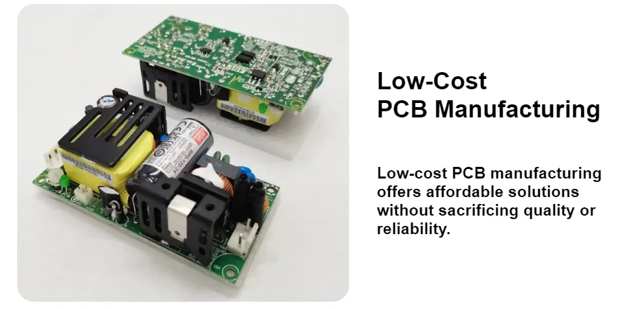
- Low Cost PCB Manufacturing: Definition and Scope
- Low Cost PCB Manufacturing Rules and Specifications
- Low Cost PCB Manufacturing Implementation Steps
- Low Cost PCB Manufacturing Troubleshooting
- 6 Essential Rules for Low Cost PCB Manufacturing (Cheat Sheet)
- FAQ
- Request a Quote / DFM Review for Low Cost PCB Manufacturing
- Conclusion
In the world of electronics hardware, "low cost" does not mean "low quality." True low cost pcb manufacturing is the result of rigorous Design for Manufacturing (DFM) engineering—optimizing your board layout to fit within the "standard capabilities" of the fabrication house to maximize yield and minimize manual handling. As Senior CAM Engineers at APTPCB, we see thousands of designs where simple tweaks to track width, hole size, or material selection could reduce production costs by 30% or more without compromising signal integrity.
Quick Answer
Low cost pcb manufacturing is achieved by designing boards that utilize standard FR4 materials, standard processing windows (e.g., track/space ≥ 5mil), and efficient panel utilization. It avoids "cost adders" like blind/buried vias, non-standard stackups, or tight tolerance requirements unless absolutely necessary.
- Golden Rule: Stick to the "Standard Spec" window (e.g., 1.6mm thickness, 1oz copper, Green solder mask) to avoid custom engineering fees.
- Common Pitfall: Specifying tight mechanical tolerances (e.g., ±0.05mm routing) or advanced via structures (HDI) on simple boards, which forces the use of expensive laser drilling and specialized alignment equipment.
- Verification: Always run a DFM check to ensure your panel utilization is above 80%; waste material is a primary driver of unit cost.
Highlights
- Material Standardization: Using widely available FR4 (TG150) eliminates special order fees and lead times.
- Layer Count Discipline: Reducing a design from 6 layers to 4 layers can drop the base price by roughly 30-40% due to fewer lamination cycles.
- Drill Efficiency: Minimizing the number of different drill bit sizes reduces tool change time and machine wear.
- Surface Finish: HASL (Hot Air Solder Leveling) remains the most cost-effective finish for general electronics, while ENIG is the standard for flat-surface requirements.
- Volume Scaling: Costs drop significantly when moving from prototype to mass production PCB manufacturing due to setup fee amortization.
Low Cost PCB Manufacturing: Definition and Scope
To understand low cost pcb manufacturing, one must understand the cost structure of a PCB factory. The price of a printed circuit board is driven by three main factors: Material Area, Process Complexity, and Yield.
- Material Area: You pay for the entire production panel (e.g., 18"x24"), not just your individual board. If your design has an odd shape that results in 50% waste on the panel, your effective cost doubles.
- Process Complexity: Every step added to the standard flow increases cost. A standard 2-layer board goes through drilling, plating, etching, and masking. If you add blind vias, the board must be drilled, plated, and laminated multiple times (sequential lamination), drastically increasing machine time and labor.
- Yield: This is the hidden cost driver. If you design with 3mil/3mil trace/space, the factory might have a 90% yield. If you design with 5mil/5mil, the yield might be 99%. The factory prices the board to cover the expected scrap rate.
Therefore, low cost manufacturing is about designing for high yield and standard processes. It involves selecting FR4 PCB materials that are stocked in bulk and avoiding features that trigger "advanced" fabrication lines unless the circuit physics demand it.
Tech / Decision Lever → Practical Impact
| Decision Lever / Spec | Practical Impact (Yield/Cost/Reliability) |
|---|---|
| Trace/Space Width | ≥ 5mil (0.127mm) ensures high yield using standard etching. < 4mil requires LDI (Laser Direct Imaging) and stricter QC, increasing cost by 15-25%. |
| Minimum Drill Size | ≥ 0.3mm allows mechanical drilling. < 0.2mm often requires laser drilling or advanced mechanical drilling, slowing production speed significantly. |
| Solder Mask Color | Green is the industry standard. It cures fastest and is printed in the highest volumes. Other colors (Red, Blue, Black) often incur batching delays or setup fees. |
| Surface Finish | HASL (Leaded) is cheapest. ENIG adds cost but ensures flat pads for BGA. Immersion Silver is a mid-range option for RF but has shorter shelf life. |
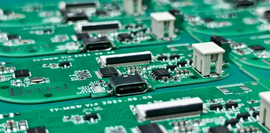
Low Cost PCB Manufacturing Rules and Specifications
Adhering to specific design rules is the most effective way to control costs. These rules ensure your board stays on the "standard conveyor belt" rather than being pulled aside for special handling.
| Rule Category | Recommended Value (Low Cost) | Why it matters | How to verify |
|---|---|---|---|
| Layer Count | 2, 4, or 6 Layers | Standard stackups are batched together. Odd layer counts (e.g., 3 or 5) are manufactured as the next even number (4 or 6) but with wasted copper etching. | Check Stackup Manager in EDA tool. |
| Board Thickness | 1.6mm (0.062") | This is the most common core thickness. Thinner (0.8mm) or thicker (2.0mm+) requires specific core inventory. | Measure board profile in 3D viewer. |
| Copper Weight | 1oz (35µm) | Standard stock. 2oz+ requires heavy copper etching protocols and wider spacing rules. | Review stackup definition. |
| Via Type | Through-Hole Only | Blind and Buried vias require sequential lamination (multiple press cycles), often doubling the board cost. | Check drill table for "Depth" or "Start/Stop" layers. |
| Slots/Cutouts | > 1.0mm width | Milling bits smaller than 1.0mm break easily and run slower. | Measure slot width in mechanical layer. |
| Panelization | V-Score preferred | V-scoring allows zero spacing between boards, maximizing panel usage compared to tab-routing which requires gaps. | View PCB fabrication process guidelines. |
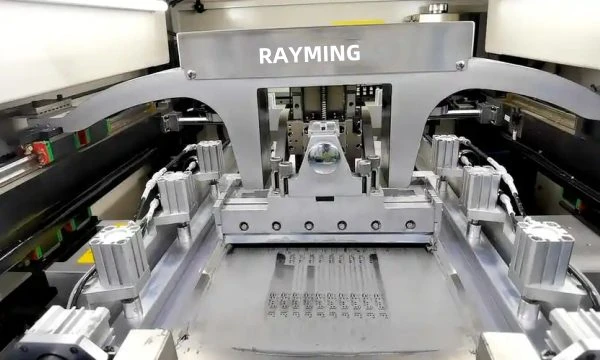
Low Cost PCB Manufacturing Implementation Steps
Implementing a cost-effective strategy requires action at the schematic and layout phase, not just at the purchasing phase.
Implementation Process
Step-by-step execution guide
Before routing, determine if you truly need 6 layers. Can optimized placement allow for 4 layers? Stick to standard dielectric thicknesses (e.g., Prepreg 7628 or 2116) to avoid custom impedance charges.
Set your EDA tool's DRC (Design Rule Check) to 5mil/5mil trace/space and 0.3mm min hole. Only violate these in specific dense areas (like under a BGA) if absolutely necessary.
Design your board shape to tessellate or fit efficiently on a standard working panel (typically 18"x24" or 21"x24"). Use V-cut (scoring) for rectangular boards to eliminate waste between units.
Submit Gerber files for a [DFM guideline](/en/resources/dfm-guidelines) check. We look for "acid traps," slivers, and isolated copper that might cause yield loss, allowing you to fix them before pricing is finalized.
Low Cost PCB Manufacturing Troubleshooting
Even with a low-cost design intent, issues can arise that drive up the final price or cause delays. Here is how to troubleshoot common friction points.
1. High Scrap Rate (Yield Loss)
If your quote is higher than expected, check your Annular Ring size. If you use a 0.3mm via with a 0.4mm pad, the annular ring is only 0.05mm (2mil). This is extremely tight for mechanical drilling registration.
- Fix: Increase via pads to at least 0.15mm (6mil) larger than the drill hole (e.g., 0.3mm drill / 0.45mm pad).
2. Board Warpage
Using a thin board (e.g., 1.0mm) with uneven copper distribution (e.g., a solid ground plane on the bottom and sparse traces on top) causes bowing during reflow. This ruins assembly yield.
- Fix: Use "Copper Thieving" (hatching) on open areas to balance the copper density between top and bottom layers.
3. Solder Mask Slithers
Designing very narrow bridges of solder mask between pads (e.g., between fine-pitch IC pins) often leads to the mask peeling off or not adhering.
- Fix: If the space between pads is less than 4mil, define the mask as a "gang opening" (one large opening for a row of pins) rather than individual openings.
6 Essential Rules for Low Cost PCB Manufacturing (Cheat Sheet)
| Rule / Guideline | Why It Matters (Physics/Cost) | Target Value / Action |
|---|---|---|
| Standard Material (FR4) | Specialty materials (Rogers, Polyimide) have high MOQ and waste costs. | FR4 TG150 |
| Trace/Space Width | Tighter spacing reduces etching yield and requires slower inspection. | ≥ 5mil / 5mil |
| Minimum Drill Size | Small drills break often and limit stack height (stack drilling). | ≥ 0.3mm (12mil) |
| Surface Finish | Gold (ENIG) involves expensive chemistry. HASL is purely mechanical. | HASL (Lead-free or SnPb) |
| Solder Mask Color | Green is printed in continuous batches. Other colors require line stops/cleaning. | Green |
| Panel Utilization | You pay for the waste. Poor nesting increases unit cost. | > 80% Efficiency |
FAQ
Q: Does "low cost" mean the PCB will fail sooner?
A: No. In fact, standard "low cost" specs (wider traces, larger vias) are often more robust and reliable than high-tech, high-density designs because they are less sensitive to manufacturing variations.
Q: Which surface finish is the absolute cheapest?
A: HASL (Hot Air Solder Leveling) with lead is generally the cheapest, followed by Lead-Free HASL. OSP (Organic Solderability Preservative) is also very cheap but has a shorter shelf life and is sensitive to handling.
Q: How much does the solder mask color affect price?
A: While the material cost difference is negligible, the process cost varies. Green is standard. Choosing Matte Black or Purple can add 10-20% to the lead time or cost for small batches because the factory has to stop the line, clean the screens, and switch inks.
Q: Can I use low cost manufacturing for impedance controlled boards?
A: Yes, but you must stick to standard stackups. If you require a specific impedance that forces the factory to use a non-standard prepreg thickness or core, the cost will rise. Use our impedance calculator to find a match with standard materials.
Q: What is the best way to get a quote?
A: Visit our quote page and upload your Gerbers. Ensure you specify "Standard Spec" where possible to see the most competitive pricing.
Request a Quote / DFM Review for Low Cost PCB Manufacturing
Ready to optimize your production costs? Send your design to APTPCB for a comprehensive DFM review. We will highlight cost-drivers and suggest alternatives.
Please provide:
- Gerber Files: RS-274X format preferred.
- Fabrication Drawing: Specifying material (FR4), thickness (1.6mm), and finish.
- Quantity: Prototype (5-100) vs. Mass Production (1000+) pricing differs significantly.
- Panelization Requirement: Let us know if you need us to panelize it for you (V-cut or Tab-route).
Conclusion
Low cost pcb manufacturing is not about cutting corners; it is about smart engineering. By aligning your design with the sweet spot of fabrication capabilities—standard materials, robust geometries, and efficient panelization—you can achieve significant cost savings while actually improving the reliability of your product.
At APTPCB, we help customers navigate these trade-offs every day. Whether you are scaling an IoT device or prototyping a consumer gadget, the principles of DFM are your best tool for cost control.
Signed, The Engineering Team at APTPCB