
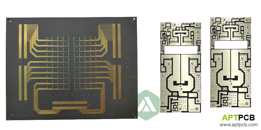
Selecting a low loss high frequency PCB requires more than choosing a laminate with a low loss tangent. RF, microwave, satellite, radar, 5G, and test equipment applications depend on the complete signal path: dielectric performance, copper profile, transmission line geometry, fabrication accuracy, and electrical verification.
A PCB material with excellent RF properties can still fail to meet system insertion loss targets when copper roughness, impedance variation, layer transitions, or manufacturing tolerances are not controlled.
This guide provides an engineering selection framework for low loss high frequency PCBs, including material comparison, copper selection, design considerations, supplier evaluation, and verification requirements.
APTPCB manufactures low loss high frequency PCBs using specialized RF materials, controlled fabrication processes, and RF-focused engineering support. Related requirements are covered in our RF high frequency PCB manufacturing resources.
What factors determine low loss high frequency PCB performance?
A low loss PCB must control every major source of attenuation in the transmission path.
| Loss source | Engineering impact | Selection or control method |
|---|---|---|
| Dielectric loss | Converts RF energy into heat and increases insertion loss | Select laminate based on Dk and loss tangent at operating frequency |
| Conductor loss | Resistive loss increases as frequency rises | Select appropriate copper thickness and profile |
| Copper roughness loss | Surface texture increases current path length because of skin effect | Specify low-profile copper when loss budget requires it |
| Radiation loss | Energy escapes from poorly controlled structures | Select suitable transmission line geometry and spacing |
| Via transition loss | Discontinuities create reflections and resonance | Optimize vias, transitions, and backdrilling requirements |
The correct PCB solution begins with a system loss budget. Frequency, trace length, bandwidth, environmental conditions, and qualification requirements determine how aggressively each parameter must be controlled.
How should engineers select low loss PCB materials?
The best laminate depends on the application, not only the lowest published loss number.
| Material category | Typical application | Selection considerations |
|---|---|---|
| PTFE laminates | Microwave, satellite, precision RF systems | Very low dielectric loss but requires specialized processing |
| Ultra-low loss PTFE | Maximum signal preservation applications | Higher cost justified by strict attenuation targets |
| Ceramic-filled PTFE | RF power and thermal-sensitive designs | Balances electrical and thermal performance |
| Hydrocarbon-based laminates | Cost-sensitive RF applications | Practical low loss performance with easier processing |
| Specialty low loss materials | Advanced microwave and millimeter-wave designs | Selected for specific electrical requirements |
Material selection should include:
- dielectric constant (Dk) at the operating frequency;
- dissipation factor (Df or tan δ);
- dielectric stability over temperature;
- dimensional stability;
- compatibility with fabrication processes;
- availability and production supply requirements.
For example, a material selected for a narrow-band radar filter may prioritize dielectric stability, while a communication backplane may prioritize manufacturability and controlled impedance consistency.
PTFE and other RF laminates require specialized fabrication knowledge because drilling, bonding, plating, and lamination processes affect final electrical performance.
APTPCB supports low loss material processing for applications including microwave RF PCB requirements.
How should copper roughness be selected for high frequency PCB designs?
Copper selection directly affects RF performance because high-frequency current flows near the conductor surface through the skin effect.
When copper surface roughness approaches the current penetration depth, the current follows the peaks and valleys of the copper surface. This increases the effective conductor path and raises insertion loss.
| Copper option | General characteristics | Typical application |
|---|---|---|
| Standard electrodeposited copper | Higher roughness, economical | Lower-frequency designs where loss margin allows |
| Low-profile copper | Reduced surface variation | General high-frequency applications |
| Very low profile copper | Lower conductor loss | Sensitive RF and microwave paths |
| Rolled annealed copper | Very smooth surface | Specialized low-loss applications |
Copper selection should consider:
- operating frequency;
- trace length;
- allowable insertion loss;
- transmission line type;
- surface finish;
- fabrication capability.
A low-loss laminate paired with unsuitable copper can produce disappointing results because conductor loss may become a significant portion of total attenuation.
What transmission line design choices reduce PCB insertion loss?
Material and copper decisions establish the foundation, but layout determines whether the design maintains predictable RF performance.
Which PCB transmission structure should be used?
Microstrip and stripline structures provide different advantages.
- Stripline provides stronger electromagnetic containment and can reduce radiation effects.
- Microstrip simplifies component access and assembly but requires careful control of field interaction and spacing.
The selection depends on frequency, mechanical constraints, assembly approach, and system architecture.
How can designers reduce RF discontinuities?
Low loss layouts typically include:
- short critical RF paths;
- minimized layer transitions;
- optimized via structures;
- controlled impedance routing;
- reduced via stub effects where required.
Every connector, transition, and discontinuity introduces potential mismatch and additional loss.
APTPCB supports controlled impedance high frequency PCB requirements through fabrication controls and engineering review.
What supplier evidence should be requested for a low loss PCB project?
Supplier evaluation should focus on demonstrated capability rather than material availability alone.
| Evaluation area | Supplier question | Evidence to request |
|---|---|---|
| Material capability | Can the supplier process the required RF laminate? | Material handling information and process experience |
| Copper control | Can copper profile requirements be maintained? | Copper specifications and process records |
| Impedance control | How is impedance verified? | Test coupon results and impedance reports |
| RF testing | Can insertion loss be measured? | VNA testing methodology and reports |
| Traceability | Can production variables be tracked? | Manufacturing records and inspection data |
| Engineering support | Can RF risks be reviewed before production? | DFM feedback and stackup review |
A qualified supplier should clearly define responsibilities:
- Fabrication responsibility: stackup accuracy, copper control, plating, inspection, and agreed testing.
- Design responsibility: frequency targets, loss budget, stackup requirements, and transmission structures.
- System qualification responsibility: final equipment validation under operating conditions.
What are common low loss PCB selection failure modes?
| Failure mode | Cause | Result |
|---|---|---|
| Selecting only by dielectric loss | Copper and geometry are ignored | Actual insertion loss exceeds simulation |
| Using unsuitable copper profile | Roughness not considered at high frequency | Increased conductor loss |
| Incorrect Dk value in simulation | Datasheet value does not match design method | Impedance variation |
| Insufficient verification planning | Testing added after fabrication | Performance problems discovered late |
| Poor supplier communication | Requirements are incomplete | Stackup and process conflicts |
Early alignment between PCB designer, manufacturer, and system engineer prevents these failures.
How should low loss PCB performance be verified?
Verification should match the application risk and frequency requirements.
| Verification method | Purpose | Evidence value |
|---|---|---|
| Vector network analyzer (VNA) testing | Measures insertion loss and return loss | Confirms RF performance |
| Material characterization | Confirms dielectric assumptions | Validates simulation inputs |
| TDR testing | Measures impedance consistency | Identifies transmission line variation |
| Test coupons | Represents production structures | Supports manufacturing monitoring |
| Statistical analysis | Tracks process stability | Improves production repeatability |
For critical RF systems, verification requirements should be defined before fabrication, including test structures, frequency range, acceptance criteria, and reporting format.
APTPCB supports electrical validation approaches aligned with testing quality requirements.
Which applications require low loss high frequency PCBs?
Low loss PCBs are used when preserving signal power directly affects system performance.
Satellite and communication systems
Typical applications include:
- antenna feed networks;
- receiver front ends;
- frequency conversion circuits;
- phased array modules.
Radar and sensing systems
Radar designs depend on consistent RF paths for:
- transmit efficiency;
- receiver sensitivity;
- phased array channel matching;
- high-frequency sensing.
Test and measurement equipment
Measurement systems require stable and repeatable electrical characteristics for:
- calibrated signal paths;
- controlled insertion loss;
- accurate device characterization.
For aerospace and defense programs, additional qualification evidence may be required through aerospace and defense PCB manufacturing requirements.
Complex multilayer RF structures should also consider high-frequency multilayer PCB design requirements.
What information should be included in a low loss PCB RFQ?
A complete RF PCB manufacturing request should include:
- operating frequency range;
- insertion loss target;
- PCB layer stackup requirements;
- preferred laminate;
- copper profile requirements;
- controlled impedance targets;
- critical trace dimensions;
- testing requirements;
- production volume;
- qualification documentation requirements.
A supplier response should define:
- recommended material options;
- achievable tolerances;
- available verification methods;
- manufacturing limitations;
- required design adjustments.
For supplier comparison guidance, review our high-frequency PCB manufacturer and RF circuit board manufacturing resources.
FAQ: Low Loss High Frequency PCB Selection
Does a low dielectric loss material guarantee low insertion loss?
No. Total PCB loss also depends on copper roughness, transmission line geometry, impedance control, and fabrication accuracy.
Is PTFE always the best low loss PCB material?
No. PTFE provides excellent RF performance but may not be optimal when mechanical stability, cost, thermal requirements, or manufacturing constraints dominate.
Why does copper roughness matter at high frequencies?
Higher-frequency current flows near the conductor surface. Rough copper increases the effective current path and contributes additional conductor loss.
Should every PCB receive VNA testing?
The required verification level depends on frequency, application risk, production requirements, and customer qualification needs.
Manufacturing low loss high frequency PCBs with controlled performance
A reliable low loss PCB solution combines material selection, copper control, transmission line design, fabrication discipline, and electrical verification.
The lowest-loss laminate alone does not determine final performance. The complete manufacturing approach must support the system loss budget and provide measurable evidence that the PCB meets the intended RF requirements.
APTPCB supports low loss high frequency PCB manufacturing through specialized materials, controlled fabrication processes, RF engineering review, and verification methods for demanding communication, radar, satellite, and test applications.
For RF projects requiring material evaluation, manufacturing feasibility review, or production planning, provide operating frequency, stackup requirements, loss targets, and validation needs during the RFQ process.