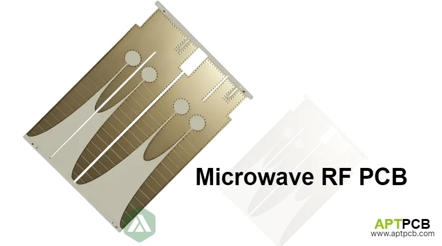
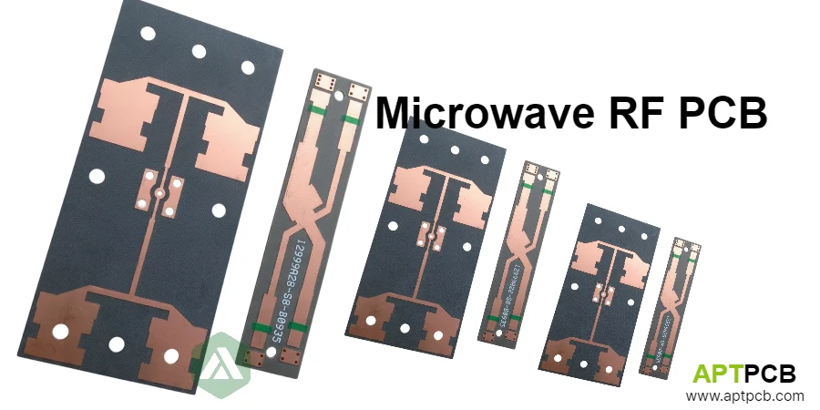
Microwave RF printed circuit boards serve applications operating from approximately 1 GHz through 100 GHz where electromagnetic wavelengths become comparable to circuit dimensions and transmission line behavior dominates electrical performance. These specialized boards form the foundation for satellite communications, phased array radar, 5G infrastructure, and automotive sensors requiring deep understanding of electromagnetic theory, advanced materials, and precision manufacturing achieving reliable high frequency performance.
At APTPCB, we manufacture microwave RF PCBs with specialized expertise implementing low-loss substrates, precision fabrication, and comprehensive RF testing. Our capabilities support RF high frequency PCB applications from L-band through millimeter-wave frequencies with validated manufacturing processes ensuring performance across demanding applications.
Understanding Microwave Electromagnetic Fundamentals
Microwave frequencies create unique design and manufacturing challenges where signal wavelengths shrink to dimensions comparable with PCB features requiring distributed circuit analysis and precise dimensional control. Understanding electromagnetic field behavior guides transmission line selection, layout practices, and mode suppression strategies. Inadequate electromagnetic understanding causes impedance discontinuities creating reflections, parasitic modes causing resonances and coupling, or radiation losses degrading efficiency — directly impacting system performance and design success.
At APTPCB, our manufacturing implements electromagnetic principles ensuring proper microwave circuit behavior.
Key Electromagnetic Considerations
- Wavelength-Dimension Relationships: At 10 GHz, wavelength in PTFE substrate shrinks to approximately 15mm making quarter-wave matching sections only millimeters long requiring precision fabrication tolerances through high frequency PCB fabrication processes.
- Distributed Circuit Behavior: Every conductor becomes a transmission line with characteristic impedance and propagation delay requiring accurate modeling through controlled impedance high frequency PCB design practices.
- Field Containment: Ground planes and shielding structures confine electromagnetic fields preventing unwanted coupling and radiation losses in high frequency multilayer PCB constructions.
- Higher Order Mode Suppression: Via fencing, substrate thickness limits, and proper grounding prevent parasitic mode propagation causing resonances above cutoff frequencies.
- Dispersion Effects: Frequency-dependent effective dielectric constant in microstrip causes velocity variation requiring consideration for wideband designs.
- Transition Management: Via transitions between layers introduce discontinuities requiring optimized anti-pad sizing, via diameter selection, and ground via placement.
Electromagnetic Design Support
Through electromagnetic understanding, validated design practices, and comprehensive manufacturing expertise coordinated with RF engineering support, APTPCB enables microwave RF PCBs achieving proper electromagnetic behavior across operating frequency ranges.
Implementing Advanced Substrate Technologies
Microwave RF PCBs require substrate materials balancing low dielectric loss with appropriate dielectric constant, thermal conductivity, dimensional stability, and manufacturing processability. Material selection critically affects insertion loss, impedance accuracy, and temperature stability. Inadequate substrate selection causes excessive signal attenuation limiting range, dielectric variations affecting impedance accuracy, or thermal management challenges limiting power handling — directly impacting system performance and application suitability.
At APTPCB, our manufacturing implements comprehensive substrate capabilities supporting demanding applications.
Key Substrate Technologies
- Low-Loss PTFE Substrates: Rogers RT/duroid 5880 and similar materials with loss tangent below 0.0009 achieving minimum insertion loss for satellite and radar applications requiring low-loss high frequency PCB performance.
- Ceramic-Filled PTFE: Rogers RO3000 series providing thermal conductivity exceeding 0.5 W/m·K while maintaining low loss for power amplifier thermal management requirements.
- Ceramic Substrates: Alumina and aluminum nitride offering exceptional dimensional stability and thermal conductivity for highest frequency and power applications.
- LTCC Technology: Low-temperature co-fired ceramic enabling complex multilayer structures with embedded passive components for compact microwave modules.
- Advanced Hydrocarbon: Rogers RO4000 series providing loss tangent around 0.003 with FR-4-like processability for cost-sensitive applications through 10 GHz.
- Material Characterization: Incoming inspection verifying dielectric constant and loss tangent ensuring material properties meet specifications through testing quality protocols.
Material Excellence
By implementing comprehensive substrate expertise, validated processing parameters, and material characterization supported by application engineering, APTPCB delivers microwave RF PCBs achieving performance requirements across substrate technologies.
Achieving Precision Transmission Line Fabrication
Microwave transmission lines including microstrip, stripline, and coplanar structures require precision fabrication maintaining impedance accuracy and minimizing losses across operating frequencies. Trace width, spacing, and dielectric thickness tolerances directly determine electrical performance. Inadequate transmission line precision causes impedance variations degrading return loss, insertion loss variations affecting gain flatness, or coupling variations impacting filter and coupler performance — significantly impacting circuit function and system performance.
At APTPCB, our fabrication implements precision processes achieving demanding transmission line specifications.
Key Transmission Line Capabilities
- Microstrip Fabrication: Precision trace width control achieving ±0.5 mil tolerance with controlled etch factor ensuring impedance accuracy on outer layer transmission lines.
- Stripline Processing: Symmetric dielectric structures with internal signal layers between ground planes achieving field containment and isolation through high frequency multilayer PCB construction.
- Coplanar Waveguide: Ground-signal-ground structures on single surfaces with precision gap control enabling probe access and simplified grounding.
- Coupled Line Structures: Edge-coupled transmission lines with controlled coupling for filter and coupler implementations requiring tight spacing tolerances.
- Via Transition Optimization: Optimized anti-pad sizing, via diameter, and ground via placement minimizing discontinuity effects through backdrilling for stub removal.
- Impedance Verification: TDR testing of production coupons confirming achieved impedance values meet specifications through high frequency PCB manufacturer quality practices.
Transmission Line Excellence
Through precision etching, controlled dielectric fabrication, and comprehensive impedance verification coordinated with field solver analysis, APTPCB achieves transmission line quality supporting demanding microwave circuit performance requirements.
Supporting Complex Microwave Circuit Integration
Microwave RF PCBs integrate passive distributed circuits with active devices including amplifiers, mixers, oscillators, and switches requiring careful attention to matching networks, bias circuits, and thermal management. Proper integration preserves device performance while enabling system functionality. Inadequate integration causes amplifier instability from improper termination, mixer conversion loss from impedance mismatches, or oscillator phase noise degradation from inadequate grounding — directly impacting system performance and operational reliability.
At APTPCB, our manufacturing supports comprehensive microwave circuit integration.
Key Integration Capabilities
- Matching Network Implementation: Distributed matching using transmission line sections achieving optimized impedance transformation for amplifier and mixer ports.
- Bias Network Fabrication: Quarter-wave bias tees and RFC structures providing DC paths while presenting appropriate RF impedances for active device operation.
- Ground Via Implementation: Dense via arrays providing low-inductance grounding for active devices with via fencing containing electromagnetic fields.
- Thermal Via Arrays: Via patterns beneath power devices transferring heat to ground planes or heat sinks supporting continuous high-power operation.
- Component Mounting: Precision pad designs accommodating surface mount and bare die components with high frequency PCB assembly compatibility.
- Shield Integration: Shield can footprints with proper ground connections enabling localized shielding of sensitive circuits.
Integration Excellence
By implementing comprehensive circuit fabrication, thermal management, and assembly-ready designs coordinated with active device requirements, APTPCB enables successful microwave circuit integration across demanding applications.
Manufacturing for Phased Array Applications
Phased array radar and communication systems require numerous identical microwave modules with consistent performance for proper array operation. Manufacturing must achieve tight parameter distributions across high volumes while maintaining quality and delivery. Inadequate manufacturing consistency causes array calibration difficulties, increased system complexity compensating for module variations, or performance degradation from outlier modules — significantly impacting array performance and system cost.
At APTPCB, our manufacturing supports phased array production requirements.
Key Phased Array Manufacturing Capabilities
- Parameter Consistency: Statistical process control maintaining tight impedance, loss, and phase distributions across production lots for array module uniformity.
- Volume Production: Scalable manufacturing capacity supporting phased array quantities with consistent quality from panel to panel.
- Module Construction: Multilayer fabrication integrating antenna elements, transmit/receive circuits, and control interfaces in compact module formats.
- Thermal Management: Effective heat dissipation structures handling power density in tightly-packed array configurations through RF circuit board manufacturing thermal design.
- Comprehensive Testing: Automated test systems verifying module performance efficiently supporting volume requirements.
- Quality Documentation: Complete traceability and statistical data supporting array integration and quality requirements through aerospace defense standards.
Phased Array Excellence
Through consistent manufacturing, statistical process control, and comprehensive testing supported by volume capability, APTPCB enables phased array module production meeting demanding performance distribution requirements.
Addressing Millimeter-Wave Manufacturing Challenges
Millimeter-wave frequencies from 30-100 GHz including 77 GHz automotive radar and emerging 5G systems impose severe requirements on substrate materials and fabrication precision. Extremely short wavelengths enable compact designs while demanding exceptional manufacturing accuracy. Inadequate millimeter-wave capability causes excessive insertion loss limiting range, dimensional errors causing frequency shifts, or surface roughness degrading performance — directly limiting addressable frequency range and applications.
At APTPCB, our manufacturing implements millimeter-wave capable processes.
Key Millimeter-Wave Capabilities
- Low-Loss Substrates: Ultra-low loss materials with loss tangent below 0.001 minimizing signal attenuation at millimeter-wave frequencies.
- Precision Etching: Advanced imaging and etching achieving trace width tolerances supporting millimeter-wave impedance requirements.
- Smooth Copper: Rolled annealed and reverse-treated foils minimizing surface roughness impact on conductor loss where skin depth approaches roughness dimensions.
- Surface Finish Selection: RF-optimized finishes avoiding magnetic losses from nickel underlayers affecting performance at millimeter-wave frequencies through RF microwave PCB expertise.
- Backdrilling Precision: Via stub removal to minimal lengths supporting frequencies through Ka-band and beyond.
- RF Testing: Network analyzer verification through millimeter-wave frequencies validating fabrication performance.
Millimeter-Wave Excellence
By implementing precision materials, fabrication processes, and testing coordinated with millimeter-wave requirements, APTPCB enables microwave RF PCBs supporting emerging high-frequency applications in automotive radar, 5G, and satellite communications.