mmWave module SMT process quick answer (30 seconds)

The mmWave module SMT process requires significantly tighter tolerances than standard SMT due to the short wavelengths (1mm–10mm) involved. Even minor physical deviations in solder volume or component alignment can cause severe signal degradation or frequency shifts.
- Placement Accuracy: Must be maintained within ±10µm to ±25µm; standard ±50µm is often insufficient for mmWave signal paths.
- Solder Voiding: Signal pad voids must be kept under 5% (area) to prevent impedance discontinuities; ground pad voids under 15% for thermal management.
- Stencil Design: Requires electro-polished or nano-coated stencils with strict aperture reduction (typically 1:0.8 or 1:0.75) to prevent solder bridging on fine-pitch components.
- Reflow Profile: A linear profile or optimized soak zone is critical to minimize voiding in LGAs and BGAs used in mmWave modules.
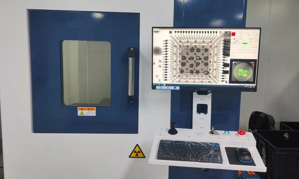
- Inspection: 100% SPI (Solder Paste Inspection) and X-Ray are mandatory; visual AOI cannot detect critical solder joint anomalies under RF shields or bottom-terminated components.
- Material Handling: Moisture Sensitivity Level (MSL) control is stricter as moisture expansion during reflow can crack sensitive high-frequency laminates.
When mmWave module SMT process applies (and when it doesn’t)
Understanding when to apply ultra-precision SMT protocols versus standard assembly helps balance cost and performance.
Apply strict mmWave SMT process when:
- Frequency exceeds 24 GHz: Applications like 5G FR2, 77GHz automotive radar, or 60GHz WiGig require precise geometry to maintain signal integrity.
- Using bare die or Flip-Chip: Direct attach methods on the module substrate demand semiconductor-grade placement accuracy.
- Components are 0201 or smaller: The stencil design for 0201/01005 passives in RF matching networks is critical for tuning.
- Modules use Cavity PCBs: Assembly involves placing components into recessed cavities, requiring specialized pick-and-place nozzle clearance and Z-axis control.
- Antenna-in-Package (AiP): The antenna elements are integrated, meaning any assembly misalignment directly detunes the radiation pattern.
Standard SMT process is sufficient when:
- Sub-6 GHz frequencies: Standard LTE, Wi-Fi (2.4/5GHz), and IoT devices generally tolerate standard IPC Class 2 variances.
- Digital-only sections: Power management or digital control logic on the same board (away from the RF front end) does not need ±10µm accuracy.
- Connectorized modules: If the mmWave function is fully contained in a pre-certified metal can module that is simply soldered onto a main board (though the module itself required the process).
- Prototyping for logic verification: If you are only testing the digital interface and not characterizing RF performance.
mmWave module SMT process rules and specifications (key parameters and limits)

The following parameters define the success of the mmWave module SMT process. Deviating from these ranges often results in functional failures that cannot be reworked.
| Rule | Recommended Value/Range | Why it matters | How to verify | If ignored |
|---|---|---|---|---|
| Placement Accuracy (X/Y) | ±10µm to ±25µm (3σ) | Misalignment alters transmission line impedance and coupling. | Post-reflow AOI / X-Ray | Signal loss, frequency shift. |
| Placement Force | 1.5N – 3.0N (component dependent) | Excessive force cracks fragile ceramic substrates or deform bumps. | Z-axis force feedback logs | Cracked die, open circuits. |
| Solder Paste Type | Type 4.5 or Type 5 (SAC305) | Smaller powder spheres are needed for fine pitch and 01005 pads. | Paste jar label / SPI | Insufficient release, grainy joints. |
| Stencil Thickness | 80µm – 100µm | Controls solder volume to prevent bridging and excess capacitance. | Laser check / SPI volume | Shorts, parasitic capacitance. |
| Aperture Reduction | 10-25% reduction | Prevents solder balls and bridging on fine-pitch RF ICs. | Gerber/Stencil check | Solder balling, shorts. |
| Signal Pad Voiding | < 5% Area | Voids change the effective dielectric constant and impedance. | 3D X-Ray / CT Scan | High VSWR, signal reflection. |
| Ground Pad Voiding | < 15-20% Area | Grounding is crucial for noise suppression and heat dissipation. | 3D X-Ray | Thermal shutdown, noise floor rise. |
| Reflow Peak Temp | 235°C – 245°C | Ensures full wetting without damaging sensitive RF laminates. | Thermal Profiler | Cold joints or delamination. |
| Time Above Liquidus (TAL) | 45s – 75s | Allows flux volatiles to escape, reducing voids. | Thermal Profiler | High voiding, brittle joints. |
| Solder Mask Web | > 75µm (if possible) | Prevents solder bridging between pads. | PCB Incoming Inspection | Bridging, difficult rework. |
| Component Coplanarity | < 80µm | Ensures all pins contact the paste during reflow. | Part datasheet / Incoming QC | Opens (Head-in-Pillow). |
mmWave module SMT process implementation steps (process checkpoints)
Executing a robust mmWave module SMT process at APTPCB (APTPCB PCB Factory) involves strict process control at every stage.
Solder Paste Printing (SPI Mandatory)
- Action: Apply Type 4.5/5 paste using a nano-coated stencil.
- Key Parameter: Volume transfer efficiency > 90%, alignment < 10µm.
- Acceptance: SPI machine passes with no height/volume violations.
High-Precision Component Placement
- Action: Mount passives and RF ICs using high-speed, high-accuracy mounters.
- Key Parameter: Placement speed reduced to 60-70% to minimize vibration; use low-force nozzles.
- Acceptance: Visual verification of alignment before reflow (pre-reflow AOI).
Reflow Soldering (Nitrogen Environment)
- Action: Reflow in a Nitrogen (N2) atmosphere (< 1000ppm O2).
- Key Parameter: N2 prevents oxidation, improving wetting and reducing voiding significantly.
- Acceptance: Profile falls within the specific process window (soak vs. ramp-to-spike).
Flux Residue Cleaning (Critical for RF)
- Action: Wash modules to remove flux residues.
- Key Parameter: Ionic contamination < 1.56 µg/cm² NaCl equivalent.
- Acceptance: ROSE test or Ion Chromatography; flux residue absorbs moisture and alters RF properties.
X-Ray Inspection (AXI)
- Action: Inspect BGA/LGA/QFN ground and signal pads.
- Key Parameter: Void calculation per pad type (Signal < 5%, Ground < 15%).
- Acceptance: Automated pass/fail based on void percentage rules.
Shield Can Attachment
- Action: Place and solder RF shield cans (often a secondary step or selective solder).
- Key Parameter: Ensure shield grounding does not short to internal components.
- Acceptance: Visual check for shield seating and solder fillet continuity.
Functional Test & Tuning
- Action: Verify RF performance (Gain, Return Loss).
- Key Parameter: Antenna tuning and trimming may be required if performance drifts.
- Acceptance: Module passes EVM (Error Vector Magnitude) and power output specs.
mmWave module SMT process troubleshooting (failure modes and fixes)
When mmWave modules fail, the root cause is often microscopic. Use this table to diagnose issues in the mmWave module SMT process.
Symptom: High Signal Loss / Poor VSWR
- Causes: Excess solder on signal pads (capacitive loading), large voids in signal path, or component misalignment.
- Checks: X-Ray for voids; Cross-section for solder joint shape.
- Fix: Optimize stencil aperture (reduce volume); adjust reflow profile to reduce voids.
- Prevention: Tighten SPI limits; use vacuum reflow if voiding persists.
Symptom: Frequency Shift (Detuning)
- Causes: Flux residue changing dielectric constant; variation in stencil design for 0201/01005 passives causing pad geometry changes.
- Checks: Cleanliness testing; verify passive component tolerances (use 1% or tighter).
- Fix: Improve cleaning process; switch to high-precision L/C components.
- Prevention: Strict flux cleaning protocols; use RF-grade passives.
Symptom: Intermittent Performance (Thermal)
- Causes: Cracked solder joints due to CTE mismatch (ceramic module on organic PCB); Head-in-Pillow defects.
- Checks: Thermal cycling test; Dye-and-Pry test.
- Fix: Adjust reflow profile (increase TAL); consider underfill for stress relief.
- Prevention: Match CTE of substrate and component; use underfill for large BGAs.
Symptom: Short Circuits under RF Shields
- Causes: Solder wicking up the shield wall; shield placement shifting during reflow.
- Checks: X-Ray (tilted view).
- Fix: Reduce paste volume on shield pads; use fixture to hold shield.
- Prevention: Design shield pads with solder dams; use segmented paste printing.
Symptom: Gain Variation across Batch
- Causes: Inconsistent solder volume on ground paddle (affecting grounding inductance).
- Checks: SPI data analysis (Cp/Cpk of paste volume).
- Fix: Clean stencil more frequently; check squeegee pressure.
- Prevention: Implement real-time SPI feedback to printer.
Symptom: Component Cracking (Capacitors)
- Causes: Excessive placement force; board flexing during depanelization.
- Checks: Microscopic inspection of component top/sides.
- Fix: Calibrate Z-axis force; use router depaneling instead of V-cut.
- Prevention: Soft-landing nozzle settings; stress-free handling.
How to choose mmWave module SMT process (design decisions and trade-offs)
Successful assembly starts with Design for Manufacturing (DFM).
- Pad Definition: Use Non-Solder Mask Defined (NSMD) pads for better registration accuracy on BGAs, but ensure the mask web is sufficient.
- Surface Finish: ENEPIG or Immersion Silver is preferred for mmWave. HASL is too uneven for fine-pitch placement and creates impedance variations.
- Grounding Vias: Place grounding vias as close to the component pad as possible (or via-in-pad) to minimize inductance, but ensure via-in-pad is filled and capped to prevent solder theft.
- Fiducials: Local fiducials are mandatory near high-frequency ICs to assist the pick-and-place machine in achieving ±10µm accuracy.
mmWave module SMT process FAQ (cost, lead time, Successful assembly starts with Design for Manufacturing (DFM) files, stackup, impedance, Dielectric Constant (DK)/Df)
1. Why is voiding such a critical issue in mmWave SMT? At mmWave frequencies, a void in a solder joint acts as a discontinuity in the transmission line, causing signal reflections and heating.
- It increases impedance unpredictably.
- It reduces the thermal transfer capability of power amplifiers.
2. Do I need Vacuum Reflow for mmWave modules? Vacuum reflow is highly recommended, especially for power amplifiers and large ground pads.
- It can reduce voiding to < 2%.
- It is essential for high-reliability aerospace or automotive radar applications.
3. Can I use standard FR4 for mmWave modules? Generally, no. Standard FR4 has high loss and inconsistent dielectric constant at > 20GHz.
- Use High Frequency PCB materials like Rogers, Taconic, or specialized Megtron.
- These materials are more stable but may require different reflow profiles.
4. How does stencil design affect 01005 components? The stencil design for 0201/01005 components requires strictly controlled area ratios (> 0.66) to ensure paste release.
- Nano-coating is often required.
- Apertures are typically reduced to prevent tombstoning and bridging.
5. Is underfill necessary for mmWave BGA components? It depends on the reliability requirement and mechanical stress.
- Underfill improves drop shock reliability.
- However, the underfill material's dielectric constant must be accounted for in the RF simulation, as it will detune the circuit.
6. What is the impact of flux residue on 77GHz radar? Flux residue is hygroscopic and can become conductive or lossy.
- At 77GHz, this causes significant signal attenuation.
- No-clean flux is often not "clean enough"; thorough washing is preferred.
7. How do you handle antenna tuning and trimming in production? While SMT places the parts, variations may require post-assembly tuning.
- Laser trimming of printed elements is one method.
- Selective placement of tuning capacitors based on initial test results is another (though costly).
8. What inspection equipment is mandatory? You cannot rely on visual inspection.
- SPI Inspection for paste volume.
- X-Ray Inspection for voids and shorts under packages.
9. How does APTPCB handle moisture sensitivity for these modules? We follow strict J-STD-033 guidelines.
- Materials are stored in dry cabinets.
- Baking is performed before reflow if exposure time is exceeded to prevent "popcorning."
10. What is the typical lead time for mmWave SMT assembly? It is longer than standard SMT due to setup and testing.
- Typically 3-5 days for assembly after kit readiness.
- DFM review takes extra time to verify high-frequency stack-ups.
11. Can you rework a mmWave module? Rework is risky and often discouraged for production units.
- Re-heating can damage the specialized laminate.
- Hand soldering cannot achieve the precision required for impedance matching.
12. What surface finish is best for wire bonding in modules? ENEPIG (Electroless Nickel Electroless Palladium Immersion Gold).
- It supports both soldering and gold wire bonding.
- It provides a flat surface for component placement.
13. How do shield cans affect the SMT process? They add thermal mass and can float if not designed correctly.
- We often use step stencils to apply more paste to shield pads.
- Clip-on shields are an alternative to avoid soldering the can directly.
mmWave module SMT process glossary (key terms)
| Term | Definition |
|---|---|
| mmWave | Electromagnetic spectrum between 30 GHz and 300 GHz (wavelength 1mm–10mm). |
| SPI | Solder Paste Inspection; 3D measurement of paste deposits before component placement. |
| Voiding | Air or flux pockets trapped inside a solder joint; critical defect in RF/Power applications. |
| Dielectric Constant (Dk) | A measure of a material's ability to store electrical energy; affects signal speed and impedance. |
| CTE | Coefficient of Thermal Expansion; the rate at which a material expands with heat. |
| 01005 / 0201 | Imperial codes for passive component sizes (01005 is 0.016" x 0.008"). |
| Skin Effect | Tendency of high-frequency current to flow only on the surface of a conductor. |
| Reflow Profile | The temperature-vs-time curve a PCB undergoes during soldering. |
| Stand-off Height | The distance between the component body and the PCB surface; affects cleaning and reliability. |
| AiP | Antenna-in-Package; integration of antenna elements directly into the IC package or module. |
| Fiducial | Optical marker on the PCB used by machines for alignment reference. |
| Underfill | Liquid encapsulant dispensed under a BGA/CSP to reduce mechanical stress. |
Request a quote for mmWave module SMT process (Successful assembly starts with Design for Manufacturing (DFM) review + pricing)
Ready to manufacture your high-frequency designs? APTPCB provides specialized DFM reviews for mmWave applications to ensure impedance control and assembly yield.
For a precise quote, please provide:
- Gerber Files (RS-274X format).
- BOM (Bill of Materials) with specific manufacturer part numbers for RF components.
- Assembly Drawings indicating orientation and special instructions (e.g., shield attachment).
- Stack-up details (Material type, Dk, Df, copper weight).
- Test Requirements (if functional test is needed).
Request a Quote Now – Get a comprehensive DFM review and pricing within 24 hours.
Conclusion (next steps)
The mmWave module SMT process is a discipline of precision, requiring tight control over stencil apertures, placement accuracy, and reflow profiles. By managing variables like stencil design for 0201/01005 components and minimizing voiding through advanced inspection, engineers can ensure the signal integrity required for 5G and radar applications. Partnering with a capable manufacturer like APTPCB ensures these stringent requirements are met from prototype to mass production.
