Definition, scope, and who this guide is for
MRI-compatible PCB materials testing is the rigorous process of validating printed circuit board substrates, copper cladding, surface finishes, and soldermasks to ensure they are non-magnetic and radio-frequency (RF) transparent within high-field magnetic resonance environments. Unlike standard electronics validation, this process focuses specifically on magnetic susceptibility, RF artifacts, and thermal safety under 1.5T, 3T, or 7T magnetic fields. The goal is to prevent image distortion (artifacts), projectile hazards, and signal-to-noise ratio (SNR) degradation.
This playbook is designed for medical device engineers, quality assurance leads, and procurement managers responsible for sourcing PCBs for MRI coils, patient monitoring systems, or in-bore electronics. It moves beyond basic theory to provide a procurement-ready framework. You will find specific material specifications, a risk assessment matrix, validation protocols, and a supplier audit checklist to ensure your manufacturing partner can deliver compliant hardware.
For teams working with APTPCB (APTPCB PCB Factory), this guide serves as a blueprint for aligning your design requirements with manufacturing capabilities. It bridges the gap between the theoretical physics of MRI compatibility and the practical realities of PCB fabrication, ensuring that the final board performs safely inside the bore without compromising diagnostic image quality.
When to use MRI-compatible PCB materials testing (and when a standard approach is better)
Deciding when to enforce strict MRI-compatible PCB materials testing depends entirely on the proximity of the electronics to the magnetic isocenter and the gradient coils.
Mandatory Testing Scenarios:
- In-Bore Devices: Any PCB located inside the scanner bore (e.g., receive coils, patient comfort displays, sensors).
- Direct Patient Contact: Devices attached to the patient during scanning, where RF heating or vibration could cause injury.
- High-Sensitivity RF Chains: Pre-amplifiers and signal processing boards where even micro-levels of ferrous contamination in the substrate can ruin SNR.
- Gradient Field Exposure: Electronics subjected to rapidly switching gradient fields, which can induce eddy currents in standard copper pours.
Standard Approach (Standard PCB) Scenarios:
- Control Room Electronics: Equipment located outside the Faraday cage (shielded room) does not require non-magnetic materials testing.
- Penetration Panel Filters: While they handle MRI signals, the external side often uses standard FR4 and standard finishes, provided the filtering is adequate.
- Low-Field Permanent Magnets: Some low-field veterinary scanners have lower sensitivity to susceptibility artifacts, though caution is still advised.
MRI-compatible PCB materials testing specifications (materials, stackup, tolerances)
Defining the correct specifications upfront prevents costly re-spins due to failed artifact tests. The following parameters must be explicitly stated in your fabrication drawing and master purchase agreement.
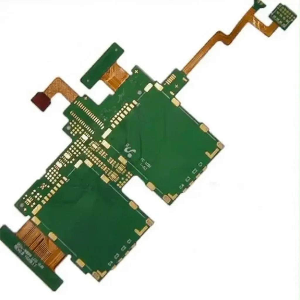
- Base Laminate (Substrate): Specify high-frequency, low-loss materials. Common choices include PTFE-based laminates (e.g., Rogers, Taconic) or non-magnetic ceramic-filled hydrocarbons. Standard FR4 is often acceptable for digital sections but must be verified for glass-weave consistency.
- Copper Foil Type: Require Rolled Annealed (RA) copper rather than Electrodeposited (ED) copper for high-frequency analog layers to minimize skin effect losses.
- Surface Finish (Critical): Explicitly ban standard Electroless Nickel Immersion Gold (ENIG) due to the ferromagnetic nickel layer. Specify Immersion Silver (ImmAg), Organic Solderability Preservative (OSP), or Electroless Palladium Immersion Gold (EPIG) if available.
- Solder Mask: Specify low-halide, non-magnetic inks. Some older green masks contain pigments with trace iron or cobalt.
- Legend/Silkscreen: Ensure inks are non-conductive and free of metallic pigments.
- Via Fill Material: If using conductive via fill, verify the silver/copper paste contains no nickel or ferromagnetic binders.
- Dimensional Stability: Maintain tighter tolerances (+/- 5%) on dielectric thickness to ensure impedance matching (usually 50Ω or 75Ω) remains stable during thermal cycling.
- Copper Thickness: Standard 1oz or 0.5oz is typical, but thickness uniformity is critical to prevent eddy current hotspots.
- Layer Registration: High-layer count boards (HDI) require registration tolerances of +/- 3 mils to maintain signal integrity in high-density coil arrays.
- Cleanliness Standards: Specify ionic contamination levels below equivalent IPC Class 3 medical standards to prevent electrochemical migration under high fields.
- Traceability: Require lot-specific Certificates of Conformance (CoC) for every material layer, down to the bonding ply.
- Testing Coupons: Include specific impedance and material test coupons on the panel rails for destructive testing.
MRI-compatible PCB materials testing manufacturing risks (root causes and prevention)
Even with perfect specs, manufacturing variables can introduce magnetic contamination. Understanding these risks allows you to implement detection gates.
- Risk: Nickel Contamination in Plating
- Root Cause: Tank cross-contamination or using a standard ENIG line by mistake.
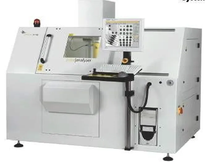
- Detection: X-Ray Fluorescence (XRF) analysis on the final finish.
- Prevention: Dedicate specific plating baths for non-magnetic orders; use Immersion Silver.
- Risk: Ferrous Residue from Drills/Routers
- Root Cause: Microscopic steel particles from drill bits embedding into the soft PTFE substrate.
- Detection: Magnified visual inspection or susceptibility testing of bare boards.
- Prevention: rigorous cleaning cycles (plasma cleaning/ultrasonic) after mechanical drilling.
- Risk: Susceptibility Artifacts (Image Distortion)
- Root Cause: Materials with magnetic susceptibility significantly different from human tissue (water).
- Detection: MRI simulation scanning of the bare board in a water phantom.
- Prevention: Match material susceptibility to tissue; avoid large solid copper planes (use cross-hatching).
- Risk: Delamination in High-Field
- Root Cause: Poor bonding between PTFE layers and copper due to thermal stress or vibration.
- Detection: Thermal shock testing and peel strength tests.
- Prevention: Use proper plasma surface treatment before lamination; select bond plies compatible with the core material.
- Risk: RF Heating (Burns)
- Root Cause: Long traces acting as antennas, coupling with the MRI transmit coil.
- Detection: Thermal camera monitoring during test scans.
- Prevention: Add RF chokes (high-impedance traps) and break up long ground loops in the design.
- Risk: Eddy Current Vibration
- Root Cause: Gradient fields inducing currents in large copper loops, causing physical vibration (acoustic noise/fatigue).
- Detection: Acoustic noise testing.
- Prevention: Slotted ground planes to break eddy current paths.
- Risk: Solder Joint Fracture
- Root Cause: Vibration from gradient switching combined with brittle solder joints.
- Detection: Vibration testing.
- Prevention: Use ductile solder alloys; underfill large components.
- Risk: Variable Dielectric Constant (Dk)
- Root Cause: Batch-to-batch variation in laminate resin content.
- Detection: TDR (Time Domain Reflectometry) impedance testing on every batch.
- Prevention: Source laminates only from Tier-1 suppliers with strict Dk control.
MRI-compatible PCB materials testing validation and acceptance (tests and pass criteria)
Validation must occur at both the laminate level and the finished PCB level.
- Magnetic Permeability Test:
- Objective: Ensure materials are non-magnetic.
- Method: ASTM A342 or low-mu permeability meter (µ < 1.01).
- Criteria: No detectable attraction to a handheld rare-earth magnet; µ must be within specified non-magnetic limits.
- RF Transparency/Loss Tangent Verification:
- Objective: Confirm signal integrity at MRI frequencies (64 MHz for 1.5T, 128 MHz for 3T).
- Method: Vector Network Analyzer (VNA) measurement of transmission lines.
- Criteria: Insertion loss must meet simulation models within +/- 0.5 dB.
- XRF Surface Analysis:
- Objective: Confirm absence of Nickel in surface finish.
- Method: X-Ray Fluorescence spectroscopy.
- Criteria: 0% Nickel content detected in the plating layer (unless specific non-magnetic Ni-alloys are used).
- Thermal Shock & Cycling:
- Objective: Verify reliability under rapid temperature changes (if used in cryo-coils).
- Method: IPC-TM-650 2.6.7.
- Criteria: No delamination, no increase in resistance >10%.
- Cleanliness (Ionic Contamination):
- Objective: Prevent corrosion and leakage currents.
- Method: ROSE testing (Resistivity of Solvent Extract).
- Criteria: < 1.56 µg/cm² NaCl equivalent.
- Solderability Test:
- Objective: Ensure the non-magnetic finish (e.g., OSP/ImmAg) accepts solder well.
- Method: Wetting balance test.
- Criteria: >95% coverage.
- Image Artifact Testing (System Level):
- Objective: Visualize distortion.
- Method: Scan the PCB in a phantom (water/oil) using standard MRI sequences (Gradient Echo).
- Criteria: Artifact size must be within defined geometric limits (e.g., < 2mm distortion).
- High-Pot / Dielectric Withstand:
- Objective: Safety isolation.
- Method: Apply high voltage between isolated nets.
- Criteria: No breakdown or arcing at specified voltage (often >1kV for coil decoupling circuits).
MRI-compatible PCB materials testing supplier qualification checklist (RFQ, audit, traceability)
Use this checklist to vet APTPCB or any other vendor for MRI-compatible PCB materials testing and fabrication.
Group 1: RFQ Inputs (What you must send)
- Material Callout: Specific laminate brand/series (e.g., "Rogers 4003C or equivalent approved").
- Non-Magnetic Requirement: Bold statement: "NO NICKEL ALLOWED IN PLATING."
- Stackup Drawing: Detailed layer stack with impedance targets.
- Gerber Files: RS-274X format with clear outline and drill files.
- Drill Chart: Distinguish between plated and non-plated holes.
- Testing Requirements: List of required IPC class (usually Class 2 or 3) and custom magnetic tests.
- Volume: Prototype vs. Production estimates.
- Surface Finish: Explicitly selected (e.g., Immersion Silver).
Group 2: Capability Proof (What they must show)
- Experience: Case studies of previous medical/MRI work.
- Equipment: VNA for impedance, XRF for material composition.
- Lamination: Vacuum lamination capabilities for mixed-dielectric boards (Hybrid FR4/PTFE).
- Etching: Fine-line etching capabilities for high-density coil arrays.
- Cleanliness: Automated washing lines capable of medical-grade cleaning.
- Certifications: ISO 13485 (Medical Devices) is highly preferred; ISO 9001 is mandatory.
Group 3: Quality System & Traceability
- Incoming QC: Do they test raw laminates for Dk/Df consistency?
- Lot Control: Can they trace a specific board back to the laminate batch and plating bath date?
- Non-Conforming Material: Procedure for quarantining magnetic-contaminated boards.
- Calibration: Are measurement tools (calipers, electrical testers) calibrated to NIST/ISO standards?
- Records: Retention of quality records for at least 5-7 years (typical for medical).
- COC: Ability to provide full Certificates of Conformance.
Group 4: Change Control & Delivery
- PCN Policy: Agreement to notify of any process change (Product Change Notification) before implementation.
- Packaging: ESD safe, vacuum sealed, with humidity indicator cards.
- Lead Time: Clear schedule for NPI vs. Mass Production.
- Logistics: Secure shipping partners.
- Communication: Dedicated account manager for technical queries.
- RMA Process: Clear policy for returns/failure analysis.
How to choose MRI-compatible PCB materials testing (trade-offs and decision rules)
Engineering is about trade-offs. Here is how to navigate the conflicting demands of MRI-compatible PCB materials testing.
- Signal Integrity vs. Cost: If you need ultra-low loss for 3T/7T receive coils, choose PTFE (Teflon) based laminates; otherwise, for 1.5T or digital control sections, choose High-Tg FR4 to save 30-50% on material costs.
- Surface Finish Durability vs. Magnetism: If you prioritize shelf life and flatness, choose Immersion Silver (non-magnetic, flat, but tarnishes); if you prioritize lowest cost, choose OSP (non-magnetic, cheap, but short shelf life); never choose standard ENIG due to nickel magnetism.
- Rigid vs. Flex: If the coil must contour to the body, choose Polyimide Flex or Rigid-Flex; otherwise, choose Rigid for better mechanical stability and lower cost.
- Thermal Conductivity vs. RF Performance: If the board carries high power (transmit coils), choose Ceramic-filled laminates for heat dissipation; otherwise, choose standard PTFE for best signal performance.
- Layer Count vs. Noise: If you need to shield sensitive signals, choose a Multilayer stackup with dedicated ground planes (cross-hatched); otherwise, choose Double-sided for simplicity and lower risk of trapped manufacturing residues.
MRI-compatible PCB materials testing FAQ (cost, lead time, Design for Manufacturability (DFM) files, materials, testing)
Q: How much does MRI-compatible PCB materials testing increase the unit cost? A: Expect a 20-50% premium over standard PCBs. This covers specialized laminates (Rogers/Taconic), non-magnetic surface finishes (Immersion Silver), and the additional overhead of XRF verification and dedicated handling to prevent ferrous contamination.
Q: What is the typical lead time for MRI-compatible PCB materials testing and fabrication? A: Standard lead time is 15-20 working days. Specialized laminates often have longer procurement cycles (up to 4-6 weeks) if not in stock, so checking material availability during the quote phase is critical.
Q: Can I use standard FR4 for MRI-compatible PCB materials design? A: Yes, but with caveats. Standard FR4 is generally non-magnetic, but you must verify the glass weave and resin do not contain magnetic impurities. It is suitable for digital logic or DC power sections but rarely used for the RF signal chain due to high dielectric loss.
Q: What specific DFM files are needed for MRI-compatible PCB materials testing? A: Beyond standard Gerbers, you must provide a fabrication drawing that explicitly forbids nickel. You should also include a "keep-out" layer for ferromagnetic components and specify cross-hatching for ground planes to minimize eddy currents.
Q: How do you perform acceptance criteria testing for magnetic susceptibility? A: The gold standard is ASTM F2052 (force test) or ASTM F2119 (artifact test). For PCB fabrication acceptance, a simple "Go/No-Go" test using a high-strength Gauss meter or a calibrated permanent magnet on the bare board is often sufficient to detect gross contamination.
Q: Why is Immersion Silver preferred over ENIG for MRI-compatible PCB materials assembly? A: ENIG (Electroless Nickel Immersion Gold) contains a layer of nickel, which is ferromagnetic and causes severe image artifacts. Immersion Silver provides a flat, solderable surface without any magnetic underlayer, making it ideal for MRI applications.
Q: Does APTPCB offer in-house MRI-compatible PCB materials testing? A: APTPCB performs material verification (XRF for composition, impedance testing). However, system-level image artifact testing (scanning the board in an MRI machine) is typically performed by the medical device manufacturer, as it requires a full scanner setup.
Q: What are the risks of skipping MRI-compatible PCB materials testing? A: Skipping testing can lead to "susceptibility artifacts" (black holes in the MRI image), heating of the device which can burn patients, or the device becoming a projectile if significant ferromagnetic material is present.
Resources for MRI-compatible PCB materials testing (related pages and tools)
- Medical PCB Manufacturing: Explore APTPCB's specific capabilities in the medical sector, including ISO 13485 compliance and reliability standards.
- High Frequency PCB: Understand the substrate options (Rogers, Taconic) essential for maintaining signal integrity in MRI RF coils.
- PCB Surface Finishes: Compare Immersion Silver, OSP, and other finishes to select the best non-magnetic option for your design.
- PCB Quality Control: Review the testing protocols, including micro-sectioning and electrical testing, that ensure your boards meet strict safety requirements.
- Rogers PCB Materials: Deep dive into the technical properties of Rogers laminates, the industry standard for high-performance MRI coil substrates.
Request a quote for MRI-compatible PCB materials testing (Design for Manufacturability (DFM) review + pricing)
Ready to validate your design? Request a Quote from APTPCB today to get a comprehensive DFM review and accurate pricing for your MRI-compatible project.
To ensure the fastest and most accurate quote, please provide:
- Gerber Files: RS-274X format.
- Fabrication Drawing: Clearly stating "Non-Magnetic / No Nickel" requirements.
- Stackup Details: Including specific laminate preferences (e.g., Rogers 4003C).
- Quantity: Prototype and production volume estimates.
- Testing Needs: Specify if you require XRF analysis reports or specific impedance coupons.
Conclusion (next steps)
MRI-compatible PCB materials testing is not just a checkbox; it is a critical safety gate that protects patients and ensures diagnostic accuracy. By rigorously defining specifications for substrates and surface finishes, understanding the risks of ferromagnetic contamination, and validating suppliers through a structured checklist, you can eliminate image artifacts and field failures. APTPCB stands ready to support your medical innovations with verified, high-precision manufacturing that meets the unique demands of the MRI environment.