Navigation Aid PCBs are the silent guardians of modern transport, functioning as the central nervous system for GPS modules, radar arrays, sonar systems, and visual beacons. Unlike standard consumer electronics, a Navigation Aid PCB must endure the harshest environments—ranging from the corrosive salt spray of the ocean to the intense vibration of aerospace applications—while maintaining zero-latency signal integrity.
For engineers and procurement managers, the challenge lies in balancing high-frequency performance with rugged durability. A failure in a Marine Navigation PCB or a Navigation Light PCB is not just a technical glitch; it is a safety hazard. APTPCB (APTPCB PCB Factory) specializes in fabricating these high-reliability boards, ensuring they meet stringent IPC Class 3 standards. This guide provides the technical specifications, implementation steps, and troubleshooting protocols necessary to deploy robust navigation electronics.
Quick Answer (30 seconds)
For engineers requiring immediate validation of a Navigation Aid PCB design, adhere to these core principles:
- Standard Compliance: Default to IPC-6012 Class 3 for manufacturing. Navigation aids are mission-critical; Class 2 is often insufficient for the vibration and thermal shock experienced in field operations.
- Material Selection: Use High-Tg FR4 (Tg > 170°C) for general logic and Rogers/Taconic laminates for RF/Radar sections to minimize signal loss.
- Surface Finish: Specify ENIG (Electroless Nickel Immersion Gold) or ENEPIG. These finishes offer superior corrosion resistance compared to HASL and provide a flat surface for fine-pitch components.
- Environmental Protection: Mandatory application of Conformal Coating (Type AR or SR) or potting compounds to prevent electrochemical migration caused by salt mist and humidity.
- Thermal Management: For
Navigation Light PCBapplications (high-power LEDs), utilize Metal Core PCBs (MCPCB) or heavy copper (2oz+) to dissipate heat effectively. - Vibration Proofing: Incorporate locking connectors and additional mounting holes near heavy components to prevent solder joint fatigue during mechanical resonance.
When Navigation Aid PCB applies (and when it doesn’t)
Understanding the operational context is vital for cost-effective design. Over-specifying adds unnecessary cost, while under-specifying risks catastrophic failure.
When to use specialized Navigation Aid PCBs
- Marine Environments: Systems exposed to saltwater, high humidity, or constant wave impact (e.g., AIS transponders, Chartplotters, Sonar transducers).
- Aviation & Aerospace: Avionics requiring resistance to rapid pressure changes and G-force loads (e.g., VOR/ILS receivers, cockpit displays).
- Outdoor Infrastructure: Land-based beacons, lighthouse controls, and remote weather monitoring stations exposed to UV radiation and rain.
- High-Frequency Applications: Radar systems and GNSS/GPS receivers where dielectric constant (Dk) stability is critical for positional accuracy.
- Safety-Critical Lighting: High-intensity LED arrays used for runway lighting or maritime signal lanterns.
When standard PCBs are sufficient (Do not use specialized specs)
- Indoor Training Simulators: Equipment used in climate-controlled office environments does not require marine-grade protection.
- Consumer Handhelds (Non-Critical): Recreational hiking GPS units where device failure does not endanger life or violate transport regulations.
- Disposable Logistics Trackers: Single-use cargo trackers where cost is the primary driver over long-term durability.
- Prototyping/Breadboarding: Initial logic verification stages where environmental stress is not yet a factor.
Rules & specifications
Designing a Navigation Aid PCB requires strict adherence to parameters that ensure longevity and signal fidelity. The following table outlines the non-negotiable rules for fabrication.
| Rule | Recommended Value / Range | Why it matters | How to verify | If ignored |
|---|---|---|---|---|
| IPC Classification | IPC-6012 Class 3 | Ensures high reliability via stricter annular ring and plating requirements. | Check fabrication drawing notes and cross-section analysis reports. | Increased risk of via failure (open circuits) under thermal cycling. |
| Base Material (RF) | Rogers 4000 / 3000 Series | Low dielectric loss (Df) is essential for Radar and GPS signal clarity. | Verify material datasheet matches stackup request; TDR testing. | Signal attenuation; reduced range or accuracy of navigation data. |
| Base Material (Logic) | High Tg FR4 (>170°C) | Prevents barrel cracking and pad lifting during high-temp assembly or operation. | Review material certification (C of C) from the laminate supplier. | Board delamination or warping during reflow or field operation. |
| Surface Finish | ENIG (2-5µin Au over 120-240µin Ni) | Provides excellent corrosion resistance and a flat surface for BGA/QFN. | X-Ray Fluorescence (XRF) measurement of plating thickness. | Black pad syndrome or rapid oxidation in saline environments. |
| Solder Mask | LPI (Liquid Photoimageable), Min 25µm | Protects copper traces from oxidation and prevents solder bridges. | Visual inspection and adhesion tape test (IPC-TM-650). | Copper corrosion; electrical shorts due to moisture ingress. |
| Via Protection | Plugged & Capped (IPC-4761 Type VII) | Prevents flux entrapment and moisture ingress into via barrels. | Microsection analysis; visual check for flat via pads. | Chemical corrosion from trapped flux; blowouts during soldering. |
| Copper Weight | 1oz (Signal), 2oz+ (Power) | Ensures sufficient current carrying capacity and mechanical strength. | Microsection analysis of copper thickness. | Overheating traces; voltage drops affecting sensor readings. |
| Cleanliness | < 1.56 µg/cm² NaCl equivalent | Ionic residues attract moisture, leading to dendritic growth. | ROSE testing (Resistivity of Solvent Extract). | Electrochemical migration causing intermittent shorts. |
| Impedance Control | 50Ω / 90Ω / 100Ω ±5% | Critical for matching RF antennas and high-speed data buses (USB/Ethernet). | TDR (Time Domain Reflectometry) coupons on production panel. | Signal reflection; data packet loss; poor GPS lock. |
| Conformal Coating | Acrylic (AR) or Silicone (SR) | Final barrier against salt spray, fungus, and humidity. | UV light inspection (if tracer is used) or thickness gauge. | Rapid corrosion of component leads and solder joints. |
| Thermal Conductivity | 1.0 - 3.0 W/mK (for MCPCB) | Essential for Navigation Light PCB to dissipate LED heat. |
Review dielectric layer specs; thermal imaging during operation. | LED overheating, color shift, and premature burnout. |
| Trace Width/Spacing | Min 4mil / 4mil (HDI) | Allows for compact designs but requires high-precision etching. | AOI (Automated Optical Inspection). | Shorts or opens if manufacturing tolerance is exceeded. |
Implementation steps

To successfully deploy a Navigation Aid PCB, follow this structured workflow. Each step includes a specific action and a validation check.
Environmental Profiling
- Action: Define the exact operating conditions. Is it a submerged sonar (IP68), a deck-mounted radar (Salt Spray + UV), or an engine room controller (Vibration + Heat)?
- Check: Document the temperature range (e.g., -40°C to +85°C) and IP rating requirements in the PRD (Product Requirements Document).
Material Selection & Stackup Design
- Action: Choose materials based on frequency and thermal needs. For a hybrid board (RF + Digital), consult APTPCB to design a stackup that combines FR4 and Rogers materials effectively.
- Check: Verify the Coefficient of Thermal Expansion (CTE) match between layers to prevent delamination.
Schematic & Layout (Signal Integrity Focus)
- Action: Route high-speed/RF signals first. Keep analog and digital grounds separate but joined at a single point (star ground) to minimize noise.
- Check: Run a DRC (Design Rule Check) for impedance constraints and ensure RF traces have adequate shielding (via stitching).
Thermal Management Design
- Action: For
Navigation Light PCBdesigns, place thermal vias under LED pads or utilize a Metal Core (Aluminum/Copper) substrate. - Check: Simulate thermal dissipation to ensure junction temperatures remain below 85% of the component's maximum rating.
- Action: For
DFM (Design for Manufacturing) Review
- Action: Submit Gerber files to the manufacturer for a DFM check. Look for acid traps, slivers, and annular ring violations.
- Check: Confirm that the manufacturer can achieve the required aspect ratio for drilling (typically 8:1 or 10:1).
Prototype Fabrication (NPI)
- Action: Produce a small batch (5-10 units) using the exact materials intended for mass production. Do not substitute materials at this stage.
- Check: Perform bare board testing (BBT) and impedance verification (TDR) before assembly.
Assembly & Coating Application
- Action: Assemble components using water-soluble or no-clean flux compatible with the chosen conformal coating. Apply coating after thorough cleaning.
- Check: Inspect coating coverage under UV light, ensuring no shadowing effects under tall components.
Environmental Stress Screening (ESS)
- Action: Subject the prototype to burn-in testing, thermal cycling, and vibration testing relevant to the marine/aviation environment.
- Check: The device must maintain full functionality without intermittent resets or signal loss during stress tests.
Failure modes & troubleshooting
Even with robust design, failures can occur. Use this guide to diagnose issues in Navigation Aid PCBs.
1. Intermittent Signal Loss (GPS/Radar)
- Symptom: Device loses lock or shows erratic position data during operation.
- Causes: Impedance mismatch, moisture absorption in dielectric, or fractured solder joints on the antenna connector.
- Checks: Perform TDR analysis on the PCB traces. Inspect RF connector soldering under a microscope.
- Fix: Re-solder connectors with flexible leads if vibration is the cause. Switch to lower moisture absorption materials (e.g., PTFE) for future revisions.
2. "Black Pad" Corrosion
- Symptom: Components pop off the board with minimal force; pads look dark or corroded.
- Causes: Hyper-corrosion of the nickel layer during the ENIG plating process (manufacturing defect).
- Checks: SEM/EDX analysis of the failed pad interface.
- Fix: This is non-repairable at the board level. The batch is suspect. Switch to ENEPIG or ensure the vendor controls the gold bath strictly.
3. LED Array Failure (Navigation Lights)
- Symptom: LEDs dim, flicker, or burn out prematurely.
- Causes: Insufficient thermal dissipation causing junction overheating.
- Checks: Measure the temperature of the MCPCB metal backing during operation. Check for voids in the thermal interface material (TIM).
- Fix: Improve heatsinking. Increase copper weight or switch to a higher conductivity dielectric (2W/mK or 3W/mK).
4. Electrochemical Migration (Dendrites)
- Symptom: Short circuits appearing over time, often visible as fern-like growths between traces.
- Causes: Ionic contamination (flux residue) combined with moisture and voltage bias.
- Checks: Visual inspection with magnification. ROSE testing for ionic cleanliness.
- Fix: Clean the PCB thoroughly using an ultrasonic bath with saponifiers. Apply a thicker or more robust conformal coating.
5. Delamination / Blistering
- Symptom: Separation of PCB layers, visible as bubbles or white patches.
- Causes: Moisture trapped inside the PCB expanding during reflow or high-temp operation.
- Checks: Check storage conditions (MSL).
- Fix: Bake PCBs before assembly (e.g., 120°C for 4 hours) to drive out moisture. Use High-Tg materials.
6. Vibration-Induced Cracking
- Symptom: Open circuits near heavy components (inductors, large capacitors) after field use.
- Causes: Mechanical resonance fatigue.
- Checks: Vibration table testing.
- Fix: Apply staking compound (RTV/Epoxy) to secure heavy components. Add mounting holes near the center of the board to increase stiffness.
Design decisions
When configuring a Navigation Aid PCB, several architectural decisions will dictate the cost and performance.
Rigid vs. Flex vs. Rigid-Flex
- Rigid PCB: The standard for most main control units and power supplies. Lowest cost and highest structural strength.
- Flex PCB: Ideal for dynamic hinge applications (e.g., folding radar wings) or fitting into compact, curved housings of handheld GPS units.
- Rigid-Flex PCB: The premium solution for complex avionics and marine instrument clusters. It eliminates connectors (a common failure point in vibration zones) by integrating the cabling into the board layers.
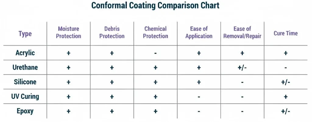
Conformal Coating Selection
- Acrylic (AR): Easy to apply and rework. Good moisture resistance but low chemical resistance. Suitable for general marine electronics.
- Silicone (SR): Excellent thermal shock and high-temperature resistance. Flexible, making it good for vibration-prone environments. Harder to rework.
- Urethane (UR): Extremely hard and chemical resistant. Best for exposure to fuels or solvents but difficult to repair.
- Parylene (XY): Vapor-deposited, ultra-thin, and pinhole-free. The gold standard for aerospace and deep-sea applications, but significantly more expensive.
RF Shielding Strategy
For navigation aids, preventing EMI (Electromagnetic Interference) is crucial.
- Board-Level Shielding: Using metal cans soldered directly over sensitive RF circuits (GPS/LNA).
- Layer Stackup Shielding: Using internal ground planes to isolate high-speed digital lines from sensitive analog antenna inputs.
- High Frequency PCB Materials: Utilizing substrates like Rogers RO4350B which maintain stable dielectric properties, reducing the need for excessive external shielding.
FAQ
Q1: What is the difference between a standard PCB and a Marine Navigation PCB? A standard PCB typically uses standard FR4 and HASL finish. A Marine Navigation PCB uses High-Tg FR4 or ceramic-filled laminates, corrosion-resistant finishes like ENIG, and requires conformal coating to survive salt spray and humidity.
- Standard: Office/Home use, 0-40°C, low humidity.
- Marine: Ocean/Outdoor use, -40 to +85°C, 100% humidity, salt fog.
Q2: Why is Impedance Control critical for Navigation Aid PCBs? Navigation systems rely on high-frequency signals (GPS at 1.575 GHz, Radar at X-band). If the trace impedance doesn't match the source and load (usually 50Ω), signals reflect back, causing data corruption and reduced detection range.
Q3: Can I use FR4 for Radar applications? Generally, no. Standard FR4 has a high Dissipation Factor (Df) which absorbs high-frequency signals. For radar (GHz range), you must use RF/Rogers materials or PTFE-based substrates to minimize signal loss.
Q4: How do I protect the PCB from salt spray? The most effective method is applying a high-quality conformal coating (Silicone or Acrylic) over the assembled board. For extreme cases, potting the entire assembly in epoxy resin provides the ultimate protection.
Q5: What is the lead time for manufacturing these specialized boards? Standard rigid boards take 3-5 days. However, Navigation Aid PCBs often require specialized materials (Rogers, Arlon) and rigorous testing (Class 3), which typically extends lead time to 10-15 days depending on material availability.
Q6: Why use a Metal Core PCB (MCPCB) for navigation lights? Navigation lights use high-power LEDs that generate significant heat. FR4 is a poor thermal conductor. Metal Core PCBs (usually Aluminum) transfer heat away from the LED 5-10 times faster than FR4, preventing burnout.
Q7: Does APTPCB support IPC Class 3 manufacturing? Yes, APTPCB is fully equipped to manufacture to IPC-6012 Class 3 standards, which is recommended for all aerospace and critical marine navigation equipment.
Q8: What files are needed for a quote? You need to provide Gerber files (RS-274X), a Drill file, a Stackup drawing (specifying material and impedance), and an Assembly drawing (if PCBA is required).
Q9: How do you test for vibration resistance? While the PCB manufacturer ensures solder joint reliability via process control, vibration testing is usually done at the assembly or system level using a shaker table to simulate specific profiles (e.g., random vibration for jet aircraft).
Q10: What is the best surface finish for wire bonding in navigation sensors? ENEPIG (Electroless Nickel Electroless Palladium Immersion Gold) is the preferred finish for wire bonding because the palladium layer prevents nickel diffusion and creates a robust bondable surface.
Q11: Can you manufacture hybrid stackups (FR4 + Rogers)? Yes, hybrid stackups are common to save cost. The RF layer uses Rogers, while the digital/power layers use cheaper FR4. This requires specialized lamination cycles which APTPCB supports.
Q12: What is the minimum trace width for these boards? For standard navigation boards, 4mil/4mil (0.1mm) is a safe standard. For advanced HDI designs in compact GPS modules, we can go down to 3mil/3mil.
Q13: How does copper thickness affect the board? Thicker copper (2oz or 3oz) handles more current and dissipates heat better but makes fine-pitch etching harder. Use heavy copper only for power distribution layers, not for fine signal lines.
Glossary (key terms)
| Term | Definition | Relevance to Navigation PCB |
|---|---|---|
| AIS | Automatic Identification System | A tracking system used on ships; requires precise RF PCB design. |
| Conformal Coating | A protective chemical film applied to PCBA. | Essential barrier against moisture, salt, and dust in marine environments. |
| CTE | Coefficient of Thermal Expansion | How much a material expands with heat. Mismatch causes reliability issues. |
| Dk (Dielectric Constant) | A measure of a material's ability to store electrical energy. | Must be stable and low for accurate Radar/GPS signal propagation. |
| Df (Dissipation Factor) | A measure of how much signal energy is lost as heat in the material. | Low Df materials (Rogers) are required for high-efficiency navigation aids. |
| ENIG | Electroless Nickel Immersion Gold | A surface finish offering flat pads and oxidation resistance. |
| GNSS | Global Navigation Satellite System | The generic term for satellite navigation (GPS, Galileo, GLONASS). |
| IPC-6012 Class 3 | Performance specification for High Reliability Electronic Products. | The manufacturing standard for equipment where downtime is not tolerated. |
| Salt Fog Test | A standardized corrosion test (ASTM B117). | Validates the effectiveness of the PCB surface finish and coating. |
| Tg (Glass Transition Temp) | The temperature where PCB material turns from rigid to soft. | High Tg (>170°C) is needed for harsh thermal environments. |
| TDR | Time Domain Reflectometry | A measurement technique used to verify the impedance of PCB traces. |
| Via Stitching | Connecting ground planes with multiple vias. | Used to shield RF traces and improve thermal performance. |
Request a quote
Ready to move your navigation system from design to deployment? APTPCB offers comprehensive DFM reviews to ensure your board meets the rigorous demands of marine and aerospace environments.
To get an accurate quote and DFM report, please prepare:
- Gerber Files: (RS-274X format preferred)
- Fabrication Drawing: Specifying IPC Class 3, material type (e.g., Rogers 4350B), and surface finish.
- Stackup Details: Layer count and impedance requirements.
- Quantity: Prototype (5-10) or Mass Production volume.
- Special Requirements: Salt spray testing, conformal coating type, or specific connector sourcing.
For complex projects involving Aerospace & Defense PCB requirements or hybrid material stackups, our engineering team is available to discuss custom solutions before you finalize your files. Visit our Contact Page for direct engineering support.
Conclusion
A Navigation Aid PCB is more than just a circuit board; it is a critical safety component that demands precision engineering and flawless manufacturing. By adhering to IPC Class 3 standards, selecting the right materials for RF and environmental stress, and implementing rigorous testing protocols, you ensure that your navigation systems perform reliably when it matters most. Whether you are designing a Navigation Light PCB for a runway or a Marine Navigation PCB for deep-sea exploration, prioritizing quality at the PCB level is the foundation of operational success.