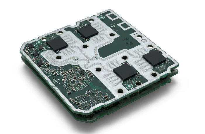
Designing hardware for Open RAN (O-RAN) networks requires strict adherence to signal integrity and thermal management standards, making a comprehensive O-RAN RU PCB guide essential for engineers. The Radio Unit (RU) in an O-RAN architecture handles the critical conversion between digital signals and radio waves, often involving Massive MIMO (mMIMO) arrays and high-power amplification. Unlike traditional proprietary base stations, O-RAN RUs must interoperate seamlessly with various Distributed Units (DUs), demanding precise impedance control and low passive intermodulation (PIM).
Acronyms used in this guide:
- Open RAN / O-RAN: Open Radio Access Network
- RU: Radio Unit
- DU: Distributed Unit
- mMIMO: Massive MIMO (Multiple-Input Multiple-Output)
- PIM: Passive Intermodulation
- eCPRI: Enhanced Common Public Radio Interface
- ENEPIG / ENIG: Surface finishes commonly specified for RF/high-reliability PCBs
This guide provides actionable specifications, manufacturing checklists, and troubleshooting steps to ensure your O-RAN RU PCB meets the rigorous demands of 5G NR deployment. APTPCB (APTPCB PCB Factory) specializes in fabricating these complex, high-frequency boards, ensuring that design intent translates perfectly to the physical product.
Quick Answer (30 seconds)
For engineers needing immediate direction on O-RAN RU PCB fabrication, here are the critical parameters to secure before starting layout or ordering prototypes:
- Material Selection: Use low-loss, high-frequency laminates (e.g., Rogers 4000 series or equivalent) for RF layers. Hybrid stackups combining high-frequency materials with high-Tg FR4 are standard to balance cost and performance.
- Layer Stackup: Expect 12 to 20+ layers for mMIMO units. Symmetrical buildup is crucial to prevent warpage during reflow, especially with mixed materials.
- PIM Mitigation: Specify "Low PIM" requirements explicitly. Use Reverse Treated Foils (RTF) or Very Low Profile (VLP) copper. Avoid HASL finishes; prefer Immersion Silver or ENEPIG.
- Thermal Management: Power Amplifiers (PAs) generate significant heat. Implement copper coin technology, heavy copper (2oz+), or dense thermal via arrays plugged with conductive epoxy.
- Impedance Control: Maintain 50Ω single-ended and 100Ω differential pairs with a tolerance of ±5% on RF lines.
- Drilling: Backdrilling is mandatory for high-speed signal vias (eCPRI interfaces) to minimize stub resonance and signal reflection.
When Open RAN (O-RAN) Radio Unit (RU) PCB guide applies (and when it doesn’t)
Understanding the scope of this O-RAN RU PCB guide ensures you apply these stringent rules only where necessary, optimizing cost and engineering effort.
When to strictly follow this guide
- 5G Massive MIMO Units: Designs incorporating 32T32R or 64T64R antenna arrays where layer-to-layer registration and crosstalk are critical.
- High-Power Radio Units: RUs operating in sub-6GHz or mmWave bands requiring active cooling or embedded copper coins for heat dissipation.
- Mixed-Signal Designs: Boards integrating RF front-ends, digital beamforming ASICs, and optical transport (eCPRI) on a single PCB.
- Interoperability Testing: When the hardware must pass O-RAN Alliance conformance tests for open fronthaul interfaces.
- Outdoor Deployments: Hardware exposed to harsh environmental conditions requiring high reliability (IPC Class 3) and specific surface protections.
When standard PCB rules suffice (and this guide is overkill)
- Digital-Only Units (DU/CU): While high-speed digital design rules apply, the specific RF material and PIM constraints of the RU are not relevant for Distributed or Central Units.
- Low-Frequency IoT Gateways: Devices operating on legacy bands (2G/3G) or simple Wi-Fi modules often do not require expensive hybrid stackups or VLP copper.
- Simple Breakout Boards: Test fixtures or connector adapters that do not carry active RF signals or high-speed data streams.
- Consumer Electronics: Standard FR4 designs for phones or laptops do not face the same thermal density or PIM requirements as infrastructure-grade RUs.
Rules & specifications
The following table outlines the non-negotiable rules for O-RAN RU PCB fabrication. These values are derived from industry best practices and APTPCB manufacturing data.
| Rule Category | Recommended Value / Range | Why it matters | How to verify | If ignored |
|---|---|---|---|---|
| Dielectric Constant (Dk) | 3.0 – 3.5 (RF Layers) | Low Dk reduces signal propagation delay and capacitive coupling in high-frequency circuits. | Review material datasheet (e.g., Rogers 4350B, Tachyon 100G). | Signal timing errors and reduced effective bandwidth. |
| Dissipation Factor (Df) | < 0.003 @ 10GHz | Minimizes signal attenuation and heat generation within the dielectric material. | VNA measurement on test coupons. | Excessive signal loss, reducing cell coverage range. |
| Copper Roughness | VLP (Very Low Profile) or HVLP | Rough copper increases skin effect losses and PIM at 5G frequencies. | SEM analysis or specifying foil type in fab notes. | High insertion loss and poor PIM performance. |
| Impedance Tolerance | ±5% (RF), ±10% (Digital) | Matches transmission lines to source/load to prevent reflections (VSWR). | TDR (Time Domain Reflectometry) testing on coupons. | High VSWR, power reflection, and potential PA damage. |
| Thermal Conductivity | > 0.6 W/m-K (Dielectric) | Ensures heat from PAs spreads laterally to thermal vias or heatsinks. | Thermal simulation and material selection. | Hotspots leading to component failure or thermal throttling. |
| Via Structure | Blind, Buried, & Backdrilled | Reduces signal stubs that act as antennas or filters at high frequencies. | Cross-section analysis (microsection). | Signal resonance, data corruption on eCPRI links. |
| Surface Finish | Immersion Silver / ENEPIG | Nickel in ENIG is ferromagnetic and causes PIM; HASL is too uneven for fine pitch. | XRF measurement for thickness and composition. | PIM failures and poor solder joint reliability on fine pitch BGAs. |
| Solder Mask | LPI, specific RF clearance | Mask over RF lines can alter impedance and increase loss. | Visual inspection and impedance re-calculation. | Unpredictable impedance shifts and increased dielectric loss. |
| Layer Registration | ±3 mil or better | Misalignment affects coupling in broadside coupled structures and striplines. | X-ray inspection of internal layers. | High crosstalk and inconsistent RF performance between batches. |
| Peel Strength | > 0.8 N/mm | High thermal stress during operation can delaminate traces, especially on PTFE materials. | Peel test per IPC-TM-650. | Trace lifting during assembly or field operation. |
| CTE (Z-axis) | < 50 ppm/°C | Prevents barrel cracks in plated through-holes during reflow and operation. | TMA (Thermomechanical Analysis). | Intermittent open circuits after thermal cycling. |
| Glass Weave Style | Spread Glass (e.g., 1067, 1078) | Prevents "fiber weave effect" where differential pairs see different Dk values. | Microsection verification. | Skew in differential pairs, degrading signal integrity. |
Implementation steps
Executing a successful O-RAN RU PCB design requires a disciplined workflow. Follow these steps to move from concept to a manufacturable board.
1. Define the Hybrid Stackup
Start by determining the layer count based on the BGA pitch of your FPGA/ASIC and the RF routing requirements.
- Action: Consult with your fabricator to define a hybrid stackup using high-frequency materials (like RF Rogers materials) for outer RF layers and high-Tg FR4 for inner digital/power layers.
- Key Parameter: Balance copper weight to prevent bowing.
- Acceptance Check: Stackup simulation confirms impedance targets are met for all signal layers.
2. Component Placement & RF Isolation
Group components by function: RF front-end, digital processing, and power management.
- Action: Place Power Amplifiers (PAs) near the edge or heat sink interfaces. Use shielding cans or fence vias to isolate RF sections.
- Key Parameter: Isolation distance > 3x trace width.
- Acceptance Check: 3D layout review shows clear separation between sensitive receiver (Rx) paths and high-power transmitter (Tx) paths.
3. Thermal Design & Coin Integration
O-RAN RUs generate massive heat. Standard thermal vias may not suffice.
- Action: Design embedded copper coins or heavy copper planes under PAs. If using vias, specify conductive epoxy filling (VIPPO).
- Key Parameter: Thermal resistance < 0.5 °C/W for the PCB path.
- Acceptance Check: Thermal simulation proves junction temperatures remain below 105°C (or specific component limit) at max load.
4. Routing & Impedance Control
Route critical RF and eCPRI lines first.
- Action: Use the impedance calculator to determine trace widths. Avoid 90-degree bends; use 45-degree or curved routing for RF.
- Key Parameter: 50Ω single-ended, 100Ω differential.
- Acceptance Check: DRC (Design Rule Check) passes with no violations on critical nets.
5. PIM Mitigation in Layout
Passive Intermodulation can degrade receiver sensitivity.
- Action: Minimize the number of vias in RF paths. Ensure ground planes are continuous and stitched thoroughly with ground vias. Avoid acute angles in copper pour.
- Key Parameter: PIM rating < -160 dBc.
- Acceptance Check: Review layout for "floating" copper islands and remove them.
6. Backdrilling Specification
Identify high-speed vias that require stub removal.
- Action: Mark vias on specific layers for backdrilling in the Gerber files.
- Key Parameter: Remaining stub length < 10 mils (0.25mm).
- Acceptance Check: Fab drawing clearly indicates backdrill depth and diameter.
7. DFM & File Generation
Before sending to production, validate manufacturability.
- Action: Run a comprehensive DFM check. Verify aspect ratios (board thickness vs. drill diameter) are within PCB manufacturing capabilities.
- Key Parameter: Min drill size 0.2mm, Aspect ratio < 10:1 (standard) or 16:1 (advanced).
- Acceptance Check: Clean Gerber/ODB++ files with no ambiguity.
8. Prototype Fabrication & Testing
Order a small batch for validation.
- Action: Send files to APTPCB. Request TDR reports and material certifications.
- Key Parameter: Lead time (typically 10-15 days for complex hybrid boards).
- Acceptance Check: Physical boards pass visual inspection and initial power-on tests.
Failure modes & troubleshooting
Even with a solid O-RAN RU PCB guide, issues can arise during testing. Use this troubleshooting framework to diagnose and fix common failures.
1. High Passive Intermodulation (PIM)
- Symptom: Reduced uplink sensitivity; noise floor rises when transmitter is active.
- Causes: Ferromagnetic materials (Nickel) in signal path, rough copper foil, poor solder joints, or loose shielding.
- Checks: Verify surface finish is Immersion Silver or ENEPIG. Check for "rusty bolt" effects in shielding cans.
- Fix: Switch to non-magnetic surface finishes. Improve solder paste volume on RF connectors.
- Prevention: Use VLP copper and avoid ENIG on RF pads.
2. Signal Attenuation (Insertion Loss)
- Symptom: Weak signal at the antenna port; PA draws excessive current to compensate.
- Causes: Wrong dielectric material, solder mask over RF lines, or excessive trace length.
- Checks: Measure trace width and dielectric thickness on a cross-section. Verify solder mask opening.
- Fix: Respin board with lower loss material (lower Df). Remove solder mask from RF traces.
- Prevention: Simulate insertion loss accurately including roughness factors before layout.
3. Thermal Shutdown
- Symptom: RU shuts down after minutes of operation; PAs overheat.
- Causes: Insufficient thermal vias, voiding in solder interface under PA, or low thermal conductivity of dielectric.
- Checks: X-ray inspection for solder voids. Verify thermal via plating thickness.
- Fix: Increase thermal via count. Use vacuum reflow to reduce voids. Implement copper coins.
- Prevention: Perform detailed thermal modeling. Use conductive epoxy filled vias (Type VII).
4. Impedance Mismatch (High VSWR)
- Symptom: Signal reflection, reduced power transfer, potential damage to transmitter.
- Causes: Etching variations, incorrect stackup height, or missing reference planes.
- Checks: TDR measurement. Check for ground plane gaps under signal traces.
- Fix: Adjust matching network components. For future spins, tighten etching tolerances.
- Prevention: Include impedance test coupons on the panel. Adhere to DFM guidelines.
5. Delamination during Reflow
- Symptom: Blisters or separation between layers, specifically between FR4 and PTFE materials.
- Causes: Moisture absorption, CTE mismatch, or improper lamination cycle.
- Checks: Check baking logs. Analyze interface between hybrid materials.
- Fix: Bake boards before assembly. Optimize lamination press cycle parameters.
- Prevention: Store PCBs in humidity-controlled environments. Choose compatible prepregs for hybrid stacks.
6. Digital-RF Crosstalk
- Symptom: Spurious emissions in the RF spectrum correlating with digital clock frequencies.
- Causes: Poor isolation, shared return paths, or lack of shielding.
- Checks: Near-field probe scanning to locate noise source.
- Fix: Add shielding cans. Improve grounding stitching.
- Prevention: Separate analog and digital grounds physically, connecting them at a single point (or use a solid common ground with careful placement).
Design decisions
Designing an O-RAN RU PCB involves trade-offs. Here is how to navigate the most common decision points.
Hybrid vs. Full High-Frequency Stackup
- Hybrid (Recommended): Uses expensive Rogers/Taconic material only for the top/bottom RF layers and standard FR4 for inner digital layers.
- Pros: Significantly lower cost, better mechanical rigidity.
- Cons: Complex lamination process, potential for warpage if not balanced.
- Full High-Frequency: Uses low-loss material for all layers.
- Pros: Best electrical performance, simple CTE matching.
- Cons: Prohibitive cost for high layer counts, mechanically soft (difficult to assemble).
Copper Coin vs. Thermal Via Array
- Thermal Vias:
- Pros: Cheap, standard process.
- Cons: Limited heat transfer capability (approx. 50-70 W/m-K effective).
- Copper Coin:
- Pros: Excellent heat transfer (380 W/m-K), direct path from component to heatsink.
- Cons: Expensive, requires precise routing and press-fit or bonding process.
- Decision: Use copper coins for PAs dissipating > 20W. Use thermal vias for drivers and LNA.
Surface Finish Selection
- ENIG: Good for flat pads but contains Nickel (bad for PIM). Avoid for RF.
- Immersion Silver: Excellent for RF (low loss, no Nickel), but tarnishes easily. Requires careful handling.
- ENEPIG: "Universal" finish. Good wire bonding, decent RF performance, but expensive.
- OSP: Cheapest, good for RF, but short shelf life and difficult for multiple reflow cycles.
- Decision: Immersion Silver is the standard for O-RAN RU PCBs due to PIM performance.
FAQ
Q1: What is the most critical factor in O-RAN RU PCB design? Signal integrity and PIM performance are paramount. The board must handle high power without distorting the signal or generating noise that deafens the receiver.
Q2: Why is backdrilling necessary for O-RAN boards? O-RAN units often use high-speed eCPRI interfaces (10Gbps/25Gbps). Vias connecting internal layers leave unused "stubs" that reflect signals. Backdrilling removes these stubs to preserve signal quality.
Q3: Can I use standard FR4 for 5G O-RAN RUs? Generally, no. Standard FR4 has high dielectric loss and unstable Dk at 5G frequencies (3.5GHz and above), leading to excessive signal loss and phase errors.
Q4: How does APTPCB handle hybrid stackup lamination? APTPCB uses optimized press cycles that account for the different curing temperatures and flow rates of FR4 and PTFE/Ceramic materials to ensure strong bonding without delamination.
Q5: What is the typical lead time for an O-RAN RU PCB? Due to the complexity and special materials, lead times are typically 10-15 working days for prototypes and 3-4 weeks for volume production.
Q6: How do I specify PIM requirements in my fabrication notes? Explicitly state: "Low PIM construction required. Passive Intermodulation < -160 dBc (2x43dBm tones). Use VLP copper and non-magnetic surface finish."
Q7: What is the best surface finish for minimizing PIM? Immersion Silver or Immersion Tin are best. OSP is also good but less robust. Avoid HASL and standard ENIG.
Q8: Does APTPCB support embedded copper coins? Yes, APTPCB supports various coin technologies, including T-coins, I-coins, and U-coins, integrated directly into the PCB for superior thermal management.
Q9: What is the maximum layer count for these boards? We regularly fabricate high-density interconnect (HDI) boards up to 40+ layers, though most O-RAN RUs fall in the 12-24 layer range.
Q10: How do I verify the impedance of my design before ordering? Use our online impedance calculator for initial estimates, but always request a stackup verification from our CAM engineers before finalizing the design.
Q11: What are the storage requirements for Immersion Silver boards? They must be stored in vacuum-sealed bags with desiccant and humidity indicator cards. They should be assembled within 6 months to prevent tarnishing.
Q12: Can you handle blind and buried vias for HDI designs? Yes, we support multiple lamination cycles for blind and buried vias, which are essential for routing dense mMIMO arrays.
Glossary (key terms)
| Term | Definition | Relevance to O-RAN RU PCB |
|---|---|---|
| O-RAN | Open Radio Access Network | The architecture defining the separation of RU, DU, and CU hardware. |
| RU (Radio Unit) | The hardware component converting digital signals to RF. | The specific device this PCB guide addresses. |
| mMIMO | Massive Multiple-Input Multiple-Output | Antenna technology using many transmitters/receivers; requires complex, high-layer-count PCBs. |
| PIM | Passive Intermodulation | Signal distortion caused by non-linearities (like magnetic metals) in the RF path. |
| eCPRI | Enhanced Common Public Radio Interface | The high-speed digital interface connecting the RU to the DU. |
| Dk (Dielectric Constant) | A measure of a material's ability to store electrical energy. | Determines signal speed and impedance; must be low and stable for RF. |
| Df (Dissipation Factor) | A measure of how much signal energy is lost as heat in the material. | Must be very low (<0.003) to prevent signal loss in 5G bands. |
| Hybrid Stackup | A PCB layup using different materials (e.g., FR4 + Rogers). | Balances the high cost of RF materials with the structural needs of the board. |
| VLP Copper | Very Low Profile Copper | Copper foil with very low roughness. |
| Backdrilling | Drilling out the unused portion of a plated through-hole. | Removes signal stubs to improve high-speed signal integrity. |
| CTE | Coefficient of Thermal Expansion | How much the material expands with heat. |
Conclusion
Successfully deploying 5G infrastructure hinges on the quality of the Radio Unit hardware. By following this O-RAN RU PCB guide, you ensure that your designs are not only electrically superior—with low PIM, precise impedance, and efficient thermal management—but also manufacturable at scale.
The transition from a digital prototype to a field-ready RF powerhouse requires a manufacturing partner who understands the nuances of hybrid materials and high-frequency physics. APTPCB brings years of experience in advanced RF fabrication to your project, ensuring your O-RAN RUs perform reliably in the most demanding networks.
Ready to validate your O-RAN design? Upload your Gerber files today for a comprehensive DFM review and accurate quotation.