Definition, scope, and who this guide is for
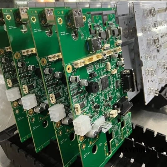
An On Board Charger PCB (OBC PCB) is the central hardware backbone responsible for converting AC grid power into DC voltage to charge the high-voltage battery pack in electric vehicles (EVs) and plug-in hybrids (PHEVs). Unlike standard automotive electronics that handle low-voltage signals (12V/24V), the OBC PCB operates in a high-voltage domain (400V to 800V+) and must manage significant thermal loads while ensuring galvanic isolation between the grid and the vehicle chassis.
This playbook is designed for automotive electronics engineers, powertrain designers, and procurement leads who are tasked with sourcing reliable PCBs for charging modules. It moves beyond basic definitions to cover the specific engineering constraints—such as heavy copper requirements, thermal management strategies, and high-voltage clearance rules—that dictate the success of the final assembly.
The decision context here is critical: a failure in an On Board Charger PCB does not just mean a non-functional accessory; it results in a vehicle that cannot charge, leading to warranty claims and safety hazards. This guide provides the technical criteria to validate designs and qualify suppliers like APTPCB (APTPCB PCB Factory) who specialize in high-reliability automotive interconnects.
When to use On Board Charger PCB (and when a standard approach is better)
Standard FR4 PCBs are insufficient for the power density required in modern EV charging. You must transition to a specialized On Board Charger PCB design when your system requirements exceed the safe operating limits of conventional materials.
Use a specialized On Board Charger PCB when:
- Voltage exceeds 400V: The dielectric breakdown voltage and Comparative Tracking Index (CTI) of standard materials may lead to arcing or carbon tracking.
- Current exceeds 30A continuous: Standard 1oz copper cannot handle the I²R losses without excessive temperature rise. Heavy copper (3oz+) or busbar integration is required.
- Thermal density is high: When power switching components (MOSFETs/IGBTs) generate heat faster than standard FR4 can dissipate, requiring Metal Core PCBs (IMS) or embedded coin technology.
- Bidirectional power flow is required: A Bidirectional Charger PCB (V2G - Vehicle to Grid) requires complex layering to handle power flow in both directions while maintaining signal integrity for control logic.
- Automotive reliability is mandated: The board must survive 15+ years of vibration, thermal shock (-40°C to +125°C), and humidity, requiring IPC-6012 Class 3 or automotive-specific adherence.
Stick to standard automotive PCBs when:
- The application is purely low-voltage control logic (e.g., the BMS monitoring circuit separate from the power path).
- Power levels are low enough (e.g., <3kW slow chargers) where standard 2oz copper and thermal vias are sufficient, avoiding the cost of heavy copper or IMS materials.
On Board Charger PCB specifications (materials, stackup, tolerances)
Defining the correct specifications upfront prevents costly engineering change orders (ECOs) during the NPI phase. Below are the baseline specifications recommended for a robust On Board Charger PCB.
- Base Material (Laminate):
- High Tg FR4 (Tg > 170°C) is the minimum standard to withstand lead-free soldering and operating temperatures.
- Anti-CAF (Conductive Anodic Filament) capability is mandatory. High voltage bias accelerates CAF growth; materials must be certified CAF-resistant.
- Comparative Tracking Index (CTI): PLC 0 or 1 (≥ 600V) to minimize electrical tracking risks on the surface.
- Copper Weight & Plating:
- Inner layers: Typically 2oz to 4oz depending on current density.
- Outer layers: 3oz to 6oz. Note that heavy copper requires wider trace spacing/gaps (etch compensation).
- Plating: ENIG (Electroless Nickel Immersion Gold) or Immersion Silver is preferred for flat pads (fine-pitch components) and wire bonding reliability.
- Stackup & Layer Count:
- Typically 4 to 12 layers.
- Power and ground planes must be adjacent to signal layers to provide shielding and reduce EMI.
- Dielectric thickness between high-voltage layers must meet breakdown voltage requirements (typically >3kV isolation).
- Thermal Management Features:
- Thermal Vias: 0.3mm to 0.5mm diameter, often plugged and capped (VIPPO) to place directly under component thermal pads.
- Metal Core (IMS): For single-layer power stages, use aluminum or copper base with high thermal conductivity dielectric (2W/mK to 8W/mK).
- Signal Integrity for Control:
- Impedance control (e.g., 90Ω differential pairs) is required for communication buses like CAN-FD or 1000BASE-T1 PCB links used for charger-to-vehicle communication.
- Solder Mask:
- Color: Green or Blue (matte finish preferred for vision systems).
- Thickness: >25µm over conductors to ensure insulation at high voltage.
- Dam size: Minimum 4mil (0.1mm) to prevent solder bridging on fine-pitch controllers.
- Dimensional Tolerances:
- Outline profile: ±0.10mm (crucial for fitting into cast aluminum housings).
- Hole position: ±0.075mm.
- Bow and Twist: <0.75% (stricter than IPC standard) to ensure flat contact with heatsinks.
- Cleanliness:
- Ionic contamination must be <1.56 µg/cm² NaCl equivalent to prevent electrochemical migration under high humidity.
On Board Charger PCB manufacturing risks (root causes and prevention)
High-voltage and high-current PCBs introduce failure modes that do not exist in standard consumer electronics. Understanding these risks allows you to audit your supplier's process effectively.
- Risk: Conductive Anodic Filament (CAF) Growth
- Root Cause: Electrochemical migration of copper along the glass fiber bundles inside the PCB dielectric, driven by high voltage bias and humidity.
- Detection: High-voltage stress testing (1000V+) in high humidity chambers.
- Prevention: Specify "CAF-resistant" materials; ensure drill hits do not fracture glass fibers excessively; maintain sufficient wall-to-wall spacing.
- Risk: Heavy Copper Undercut / Etch Traps
- Root Cause: Etching thick copper (e.g., 4oz) takes longer, causing the chemical to eat sideways (undercut) under the photoresist.
- Detection: Cross-section analysis (microsection) showing trapezoidal trace shapes reducing the effective conductor width.
- Prevention: Supplier must apply etch compensation factors to artwork; design rules must allow wider spacing for heavier copper.
- Risk: Delamination during Reflow
- Root Cause: Moisture trapped in the PCB expands rapidly at reflow temperatures (popcorning), or mismatch in CTE (Coefficient of Thermal Expansion) between layers.
- Detection: Scanning Acoustic Microscopy (SAM) or visual blistering after reflow.
- Prevention: Baking PCBs before assembly; using high-Tg, low-CTE materials; strictly controlling lamination pressure and temperature profiles.
- Risk: Solder Joint Fatigue (Thermal Cycling)
- Root Cause: The PCB expands and contracts at a different rate than the ceramic components or the aluminum heatsink, stressing solder joints.
- Detection: Thermal shock testing (-40°C to +125°C) followed by shear testing or electrical continuity checks.
- Prevention: Match CTE of PCB to components where possible; use underfill for large BGAs; ensure robust copper plating in via barrels (min 25µm).
- Risk: High Voltage Arcing (Creepage Failure)
- Root Cause: Dust, moisture, or flux residue reduces the effective insulation resistance between high-voltage traces.
- Detection: Hi-Pot testing; visual inspection of spacing.
- Prevention: Design slots (air gaps) between high-voltage nodes; apply conformal coating; ensure strict adherence to IPC-2221 clearance rules.
- Risk: Plated Through Hole (PTH) Cracking
- Root Cause: Z-axis expansion of the PCB material stresses the copper barrel during thermal cycling.
- Detection: Resistance changes during thermal cycling; cross-sectioning.
- Prevention: Use materials with low Z-axis CTE; ensure copper plating ductility and thickness (Class 3 requires average 25µm).
- Risk: Impedance Mismatch on Comms Lines
- Root Cause: Variation in dielectric thickness or trace width during manufacturing affects 1000BASE-T1 PCB signals.
- Detection: TDR (Time Domain Reflectometry) testing on coupons.
- Prevention: Tighter process controls on etching and lamination; specify impedance tolerance of ±5% or ±10%.
- Risk: Warpage preventing Heatsink Contact
- Root Cause: Unbalanced copper distribution (e.g., solid ground plane on bottom, sparse traces on top) causes bowing.
- Detection: Warpage measurement using shadow moiré or feeler gauges.
- Prevention: Copper balancing (thieving) in design; use of heavy fixtures during reflow; strict bow/twist specs (<0.5% or 0.75%).
On Board Charger PCB validation and acceptance (tests and pass criteria)

Validation must occur at both the bare board level and the assembly level. Do not rely solely on the supplier's Certificate of Compliance (CoC).
- Electrical Continuity & Isolation (100% Test):
- Objective: Ensure no opens, shorts, or leakage.
- Method: Flying probe or bed-of-nails tester.
- Criteria: Isolation resistance >100MΩ at 250V/500V; continuity <10Ω.
- Hi-Pot (Dielectric Withstand) Test:
- Objective: Verify insulation between primary (HV) and secondary (LV) sides.
- Method: Apply high voltage (e.g., 2500V DC) for 60 seconds.
- Criteria: Leakage current <1mA; no breakdown or arcing.
- Thermal Stress (Solder Float):
- Objective: Simulate soldering thermal shock.
- Method: Float sample in solder pot at 288°C for 10 seconds (IPC-TM-650).
- Criteria: No blistering, delamination, or lifted pads.
- Microsection Analysis (Coupon):
- Objective: Verify internal stackup and plating quality.
- Method: Cross-section of test coupon.
- Criteria: Copper thickness meets spec (e.g., min 25µm in holes); no inner layer separation; proper registration.
- Ionic Contamination Test:
- Objective: Ensure board cleanliness to prevent electrochemical migration.
- Method: Rose test or Ion Chromatography.
- Criteria: <1.56 µg/cm² NaCl equivalent (or customer specific limit).
- Solderability Test:
- Objective: Ensure pads will accept solder during assembly.
- Method: Dip and look / wetting balance.
- Criteria: >95% coverage of the surface; uniform wetting.
- Impedance Verification (if applicable):
- Objective: Validate signal integrity for comms lines.
- Method: TDR measurement on test traces.
- Criteria: Measured impedance within ±10% of design target.
- Dimensional Verification:
- Objective: Ensure mechanical fit.
- Method: CMM (Coordinate Measuring Machine) or optical measurement.
- Criteria: All dimensions within tolerance; hole sizes within ±0.05mm (plated).
On Board Charger PCB supplier qualification checklist (RFQ, audit, traceability)
When vetting a manufacturer like APTPCB, use this checklist to ensure they have the specific capabilities for automotive power electronics.
Group 1: RFQ Inputs (What you must provide)
- Gerber Files (RS-274X): Complete set including all copper, mask, silk, and drill layers.
- Fabrication Drawing: Specifying material (IPC-4101 sheet), class (IPC-6012 Class 3), tolerances, and finishing.
- Stackup Diagram: Explicitly defining dielectric thicknesses and copper weights (e.g., "L1 3oz, L2 2oz...").
- Netlist (IPC-356): Critical for electrical test verification against the design logic.
- Drill Chart: Distinguishing between plated and non-plated holes, and defining via types (blind/buried/through).
- Panelization Drawing: If you require specific arrays for your assembly line.
- Special Requirements: E.g., "Press-fit hole tolerance," "Edge plating," or "Specific CTI value."
- Volume & EAU: Estimated Annual Usage to determine tooling strategy.
Group 2: Capability Proof (What the supplier must show)
- IATF 16949 Certification: Mandatory for automotive supply chains. ISO 9001 is not enough.
- Heavy Copper Experience: Samples or case studies of 4oz+ copper production.
- High Voltage Testing: In-house capability for Hi-Pot and CAF testing (or a partner lab).
- Automated Optical Inspection (AOI): Must be used on all inner layers, not just outer.
- UL Listing: The specific stackup and material combination must be UL recognized (94V-0).
- Cleanliness Lab: In-house ability to test for ionic contamination.
Group 3: Quality System & Traceability
- PPAP (Production Part Approval Process): Supplier must be willing to submit Level 3 PPAP documentation.
- Traceability: Every PCB (or panel) must have a unique ID (QR/Datamatrix) linking it to the production batch, date, and material lot.
- PFMEA (Process Failure Mode Effects Analysis): Evidence that they have analyzed risks in their manufacturing process.
- Control Plan: Document detailing how critical characteristics (hole wall thickness, impedance) are monitored.
- MRB (Material Review Board): Process for handling non-conforming material (quarantine procedures).
Group 4: Change Control & Delivery
- PCN (Product Change Notification): Agreement that no changes to materials, chemicals, or location will occur without prior approval.
- Buffer Stock: Willingness to hold safety stock (VMI) to mitigate lead time fluctuations.
- Packaging: ESD safe, vacuum sealed with desiccant and humidity indicator cards (HIC).
- DDP/Incoterms: Clear agreement on shipping terms and liability transfer.
How to choose On Board Charger PCB (trade-offs and decision rules)
Engineering is about trade-offs. Here is how to navigate the key decisions for OBC PCBs.
- Heavy Copper vs. Busbars:
- If current is <50A and space is tight, choose Heavy Copper PCB (3-4oz). It integrates everything into one board.
- If current is >100A, choose Busbar integration or external wiring. Extremely thick copper (6oz+) becomes very expensive and hard to etch precisely.
- FR4 vs. Metal Core (IMS):
- If the design uses through-hole components and multiple signal layers, choose High-Tg FR4 with thermal vias.
- If the design is purely surface mount power switches (MOSFETs) needing massive heat sinking, choose Metal Core (IMS). Note that IMS is typically limited to 1 or 2 layers.
- Integrated vs. Separate Control Board:
- If you want modularity and easier noise isolation, choose Separate Boards (one Power PCB, one Control PCB connected via headers).
- If you need to minimize size and assembly steps, choose Integrated Design. This requires careful layout to isolate the 1000BASE-T1 PCB signals from high-voltage switching noise.
- Surface Finish:
- If you use aluminum wire bonding or fine-pitch BGAs, choose ENIG.
- If cost is the main driver and the environment is less harsh, choose HASL (Lead-Free), but beware of planarity issues on large pads.
- If press-fit connectors are used, choose Immersion Tin or Immersion Silver (though Silver tarnishes easily).
- Solder Mask Type:
- If voltage is very high (>800V), choose Double-coat Solder Mask or specific high-voltage dielectric coatings to prevent arcing.
On Board Charger PCB FAQ (cost, lead time, Design for Manufacturability (DFM) files, materials, testing)
Q: What is the primary cost driver for an On Board Charger PCB? A: Copper weight and material grade. Jumping from 1oz to 3oz copper can double the laminate cost, and requiring high-CTI / high-Tg automotive materials adds a premium over standard FR4.
Q: How does heavy copper affect the DFM (Design for Manufacturing) rules? A: You must increase trace spacing. For 1oz copper, 4mil spacing is standard; for 3oz copper, you typically need 8-10mil spacing to allow the etchant to clear the copper from the bottom of the gap without shorting.
Q: What is the typical lead time for automotive OBC PCBs? A: Standard lead time is 3-4 weeks for production. However, if specialized materials (like specific Rogers or high-CTI laminates) are not in stock, lead times can extend to 6-8 weeks. Quick-turn prototypes can be done in 5-7 days.
Q: Can I use standard FR4 for a 400V On Board Charger PCB? A: Generally, no. Standard FR4 may not have the required CTI (Comparative Tracking Index) or thermal reliability (Tg). You should specify "High Tg (>170°C), CTI PLC 0" material to ensure safety and longevity.
Q: What specific testing is required for Bidirectional Charger PCBs? A: Beyond standard e-test, bidirectional boards often require stricter impedance control verification for the complex control loops and potentially higher thermal cycling parameters due to the dual-mode operation heating.
Q: How do I specify acceptance criteria for "voids" in thermal pads? A: In your fabrication notes, reference IPC-A-600 or IPC-6012 Class 3. For thermal pads under power devices, you might specify "Maximum 25% voiding area" to ensure sufficient heat transfer.
Q: Why is "press-fit" technology popular in OBC PCBs? A: Press-fit connectors eliminate the need for soldering large connector pins, which can be difficult on heavy copper boards due to the massive heat sinking effect. They provide a reliable, gas-tight mechanical connection.
Q: What files are needed for a DFM review of an On Board Charger PCB? A: Send Gerber files (RS-274X), a drill file with hole plating defined, a netlist (IPC-356), and a detailed stackup drawing. Mentioning the "operating voltage" in the notes helps the CAM engineer check for clearance violations.
Resources for On Board Charger PCB (related pages and tools)
- Automotive Electronics PCB: Explore our specific capabilities for the automotive sector, including IATF 16949 compliance and reliability standards.
- Heavy Copper PCB: Deep dive into the manufacturing constraints and benefits of using 3oz+ copper for high-current charging applications.
- Metal Core PCB: Understand when to switch from FR4 to Aluminum or Copper base substrates for superior thermal dissipation.
- High Thermal PCB: Learn about material options that manage heat effectively, preventing component failure in enclosed charging modules.
- Turnkey Assembly: See how we handle the full process from bare board fabrication to component sourcing and final assembly.
- Quote Request: Ready to move forward? Use this page to submit your data for a comprehensive engineering review.
Request a quote for On Board Charger PCB (Design for Manufacturability (DFM) review + pricing)
For a precise quote and a complimentary DFM review that checks your high-voltage clearances and heavy copper spacing, submit your design data to APTPCB.
Please include the following for an accurate assessment:
- Gerber Files & Drill Data: Ensure all layers are present.
- Stackup & Material Specs: Specify copper weight (e.g., 3oz) and material Tg.
- Volume: Prototype quantity vs. Mass production EAU.
- Special Requirements: CTI value, breakdown voltage, or specific automotive standards (IPC Class 3).
Click here to Request a Quote & DFM Review
Conclusion (next steps)
Sourcing a reliable On Board Charger PCB is about managing the intersection of high power, thermal stress, and strict automotive safety regulations. By defining your specifications for heavy copper and isolation early, validating against failure modes like CAF and thermal fatigue, and auditing your supplier for IATF 16949 compliance, you de-risk your EV program significantly. Whether you are building a unidirectional unit or a complex Bidirectional Charger PCB, the right manufacturing partner ensures your design translates into a safe, durable product on the road.