Key Takeaways
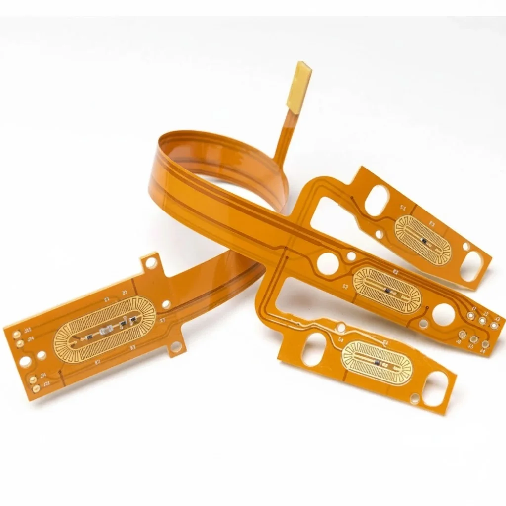
Optical sorting technology has revolutionized industries ranging from food safety to recycling by automating the separation of materials based on color, shape, and structural properties. At the heart of these machines lies the Optical Sorting PCB, a specialized circuit board designed for high-speed data processing and extreme durability.
Before diving into the technical depths, here are the critical takeaways for engineers and procurement managers:
- Speed is Non-Negotiable: These PCBs must process signals from high-resolution cameras and sensors in milliseconds to trigger air ejectors accurately.
- Signal Integrity is Critical: High-frequency signals between FPGAs and sensors require precise impedance control to prevent data loss.
- Environmental Resilience: Unlike standard office electronics, these boards often operate in dusty, vibrating, or humid environments.
- Thermal Management: High-performance processors generate significant heat, requiring advanced stackups and heat dissipation strategies.
- Validation is Key: Automated Optical Inspection (AOI) alone is insufficient; functional testing under load is mandatory.
- Holistic Design: The PCB must integrate seamlessly with mechanical ejection systems and optical sensors.
What Optical Sorting PCB really means (scope & boundaries)
To understand how to design or order an Optical Sorting PCB, we must first define its specific role within the larger machine ecosystem.
The Definition
An Optical Sorting PCB is the central processing unit and control interface for optical sorting machinery. It acts as the bridge between the "eyes" of the machine (cameras, lasers, NIR sensors) and the "hands" of the machine (pneumatic ejectors or mechanical flaps).
When APTPCB (APTPCB PCB Factory) manufactures these boards, we categorize them as high-performance industrial control boards. They differ from standard consumer electronics because they must handle massive data throughput in real-time while surviving harsh industrial conditions.
Core Functions
- Data Acquisition: Receives raw image or spectral data from CCD/CMOS sensors.
- Processing: Uses FPGAs (Field Programmable Gate Arrays) or DSPs (Digital Signal Processors) to analyze data against predefined algorithms.
- Actuation: Sends high-current pulses to solenoid valves to eject unwanted material.
- Communication: Interfaces with the user HMI (Human-Machine Interface) and upstream/downstream equipment.
Scope of Application
While the primary focus here is optical sorting, the technology shares similarities with other industrial control boards. For instance, the environmental protection required for an Optical Sorting PCB is comparable to an Activated Sludge PCB used in wastewater treatment, where moisture and corrosion resistance are paramount. Similarly, the sensor precision required mirrors that of an Aeroponic Control PCB, which monitors delicate nutrient mists in agriculture. However, the Optical Sorting PCB is unique in its demand for ultra-low latency.
Metrics that matter (how to evaluate quality)
Building on the definition of high-performance requirements, we must quantify what "quality" looks like. You cannot improve what you cannot measure.
The following table outlines the critical metrics that determine the success of an Optical Sorting PCB.
| Metric | Why it matters | Typical Range / Factors | How to Measure |
|---|---|---|---|
| Signal Latency | Delays cause the ejector to miss the target object. | < 1ms (system level); Trace length matching is critical. | Time Domain Reflectometry (TDR) & Oscilloscope. |
| Impedance Control | Mismatches cause signal reflection and data corruption. | 50Ω (Single) / 90Ω or 100Ω (Differential) ±10%. | Impedance Calculator & TDR testing. |
| Thermal Resistance | FPGAs overheat without efficient heat transfer. | Dependent on material (Tg > 170°C recommended). | Thermal imaging under load. |
| Vibration Resistance | Sorting machines vibrate constantly; solder joints can crack. | IPC Class 3 standard for reliability. | HALT (Highly Accelerated Life Test). |
| Current Capacity | Solenoid drivers require sudden high-current bursts. | 2oz to 4oz copper weight is common. | DC load testing & thermal rise monitoring. |
| Dielectric Constant (Dk) | Affects signal propagation speed. | 3.4 - 4.5 (Stable over frequency). | Material datasheet verification. |
Selection guidance by scenario (trade-offs)
Once you understand the metrics, the next step is selecting the right PCB architecture for your specific application. Not all sorting machines are created equal.
Scenario 1: Rice and Grain Color Sorters
- Requirement: Extremely high throughput, moderate resolution.
- Trade-off: Prioritize processing speed over complex spectral analysis.
- Recommendation: Use a multi-layer FR4 High-Tg board. Standard copper thickness (1oz-2oz) is usually sufficient.
- Risk: Dust accumulation can cause short circuits if not coated.
Scenario 2: Recycling (Plastic/Glass) Sorters
- Requirement: Complex material identification (NIR/Hyperspectral) and heavy mechanical ejection.
- Trade-off: Requires robust power distribution networks (PDN) to drive powerful air nozzles.
- Recommendation: Hybrid stackup using high-speed materials (like Rogers or Megtron) for the sensor layer and thick copper for the power layer.
- Risk: High vibration from heavy material impact requires reinforced mounting holes and flexible interconnects.
Scenario 3: Mining and Ore Sorting
- Requirement: Extreme durability and X-ray/Laser sensor integration.
- Trade-off: Cost is secondary to reliability. Failure means stopping a massive production line.
- Recommendation: Ceramic-based substrates or metal-core PCBs (MCPCB) for heat dissipation and rigidity. Conformal coating is mandatory.
- Risk: Abrasive dust and moisture. This environment is as harsh as the one an Activated Sludge PCB faces, requiring similar potting or coating strategies.
Scenario 4: Pharmaceutical Inspection
- Requirement: 100% accuracy, zero contamination.
- Trade-off: Speed is sacrificed for absolute precision.
- Recommendation: HDI (High Density Interconnect) boards to miniaturize the camera modules. Gold surface finish (ENIG/ENEPIG) for corrosion resistance.
- Risk: Signal noise affecting detection algorithms.
Scenario 5: Fresh Produce (Fruit/Veg) Sorting
- Requirement: Soft handling, variable shapes, humidity resistance.
- Trade-off: Sensors must detect internal rot (sugar content), requiring specific frequencies.
- Recommendation: Low-loss laminates to support high-frequency analog signals.
- Risk: High humidity environment similar to an Aeroponic Control PCB; requires water-resistant enclosures and coatings.
Scenario 6: Laboratory/Research Sorters
- Requirement: Flexibility and reprogrammability.
- Trade-off: Higher unit cost for prototyping.
- Recommendation: Standard build with socketed components for easy upgrades.
- Risk: Over-engineering for a non-production environment.
From design to manufacturing (implementation checkpoints)
Selecting the right scenario is only the beginning; executing the design requires a rigorous process. The following checklist ensures your Optical Sorting PCB moves from concept to production without costly revisions.
Phase 1: Design & Layout
High-Speed Routing:
- Recommendation: Route differential pairs for cameras first. Keep them short and direct.
- Risk: Crosstalk between sensor data and solenoid power lines.
- Acceptance: Simulation shows eye diagrams are open.
Stackup Definition:
- Recommendation: Define layer stackup early. Place ground planes adjacent to high-speed signal layers.
- Risk: EMI radiation failing compliance tests.
- Acceptance: Review with APTPCB manufacturing engineers.
Power Integrity:
- Recommendation: Use wide traces or polygons for power rails driving the ejectors.
- Risk: Voltage droop causing ejector misfires.
- Acceptance: IR Drop analysis.
Phase 2: Pre-Production (DFM)
Component Footprints:
- Recommendation: Verify footprints for FPGAs and connectors against datasheets.
- Risk: Soldering defects on BGA components.
- Acceptance: DFM Guidelines check.
Thermal Vias:
- Recommendation: Place sufficient thermal vias under hot components.
- Risk: Component throttling or failure.
- Acceptance: Thermal simulation.
Phase 3: Fabrication
Material Verification:
- Recommendation: Ensure the fab house uses the specified High-Tg or Low-Loss material.
- Risk: Delamination during reflow.
- Acceptance: Certificate of Conformance (CoC).
Impedance Testing:
- Recommendation: Test coupons on every panel.
- Risk: Signal degradation.
- Acceptance: TDR report within ±10%.
Phase 4: Assembly & Testing
Solder Paste Inspection (SPI):
- Recommendation: 100% SPI for fine-pitch components.
- Risk: Dry joints on critical processors.
- Acceptance: Zero volume defects.
Conformal Coating:
- Recommendation: Apply coating to protect against dust/moisture (except on connectors).
- Risk: Sensor interference if coating covers optical components.
- Acceptance: UV light inspection.
Functional Test (FCT):
- Recommendation: Simulate camera inputs and measure ejector output timing.
- Risk: Passing electrical tests but failing logic requirements.
- Acceptance: 100% functional pass.
Common mistakes (and the correct approach)
Even with a checklist, engineers often fall into specific traps when designing Optical Sorting PCBs.
Mistake: Ignoring the "Return Path"
- Context: High-speed signals need a clean return path on the reference plane.
- Correction: Never route high-speed traces over a split plane. Stitch ground vias near signal vias.
Mistake: Underestimating Solenoid Noise
- Context: Ejectors create massive inductive kickback (noise) when switching.
- Correction: Use flyback diodes and separate the power ground from the digital ground (connect them at a single point or use a filter).
Mistake: Selecting Standard FR4 for High Frequencies
- Context: Standard FR4 has a high Loss Tangent, absorbing high-frequency signals.
- Correction: Use specialized materials like Rogers or Isola for signal layers, or hybrid stackups to save cost.
Mistake: Neglecting Vibration Stress
- Context: Sorting machines shake. Heavy components (capacitors/inductors) can shear off.
- Correction: Use adhesive bonding (staking) for large components and choose flexible termination capacitors.
Mistake: Poor Connector Placement
- Context: Placing connectors on the edge without mechanical support.
- Correction: Use through-hole reinforcement for connectors that will be plugged/unplugged frequently.
Mistake: Overlooking Thermal Expansion
- Context: Different materials expand at different rates (CTE mismatch).
- Correction: Ensure the CTE of the BGA package matches the PCB substrate as closely as possible to prevent solder ball cracking.
FAQ
Q: What is the typical lifespan of an Optical Sorting PCB? A: In industrial environments, these boards are expected to last 5-10 years. However, this depends heavily on the quality of the conformal coating and thermal management.
Q: Can I use a standard PC motherboard for optical sorting? A: Generally, no. Standard motherboards lack the specific I/O interfaces for industrial cameras and the robust solenoid drivers required for ejection. They also lack the vibration resistance needed.
Q: How does an Optical Sorting PCB differ from an Activated Sludge PCB? A: Both require environmental protection. However, the Optical Sorting PCB prioritizes high-speed signal processing (FPGA/DDR), whereas an Activated Sludge PCB prioritizes analog sensor accuracy (pH, oxygen levels) and high-voltage relay switching for pumps.
Q: Why is FPGA preferred over MCU for these boards? A: FPGAs process data in parallel, allowing them to handle image data from multiple cameras simultaneously with near-zero latency. MCUs process sequentially, which is often too slow for real-time sorting.
Q: What surface finish is best? A: ENIG (Electroless Nickel Immersion Gold) is recommended. It provides a flat surface for fine-pitch BGAs and offers excellent corrosion resistance.
Q: Do I need blind and buried vias? A: For complex, high-density boards (HDI), yes. They allow for tighter routing and better signal integrity but increase manufacturing costs.
Q: How do I specify the impedance requirements? A: You should specify the target impedance (e.g., 100Ω differential) and the specific layers/traces in your fabrication notes. You can use our Impedance Calculator to estimate trace widths.
Q: What data do I need to send for a quote? A: Gerber files (RS-274X), BOM (Bill of Materials), Pick & Place file, and a detailed fabrication drawing specifying materials, stackup, and special requirements like impedance control.
Glossary (key terms)
| Term | Definition |
|---|---|
| AOI | Automated Optical Inspection. A camera-based check during manufacturing to find soldering defects. |
| BGA | Ball Grid Array. A type of surface-mount packaging used for high-performance processors (FPGAs). |
| CCD | Charge-Coupled Device. A type of image sensor used in high-end optical sorters. |
| CTE | Coefficient of Thermal Expansion. How much a material expands when heated. |
| Differential Pair | Two complementary signals sent on paired traces to reduce noise and improve integrity. |
| DSP | Digital Signal Processor. A specialized microprocessor optimized for the operational needs of digital signal processing. |
| EMI | Electromagnetic Interference. Disturbance generated by an external source that affects an electrical circuit. |
| FPGA | Field-Programmable Gate Array. An integrated circuit designed to be configured by a customer after manufacturing. |
| HDI | High Density Interconnect. A PCB technology that uses microvias and fine lines to pack more functionality into less space. |
| NIR | Near-Infrared. A spectral region used in sorting to identify materials based on chemical composition, not just color. |
| Stackup | The arrangement of copper layers and insulating layers in a PCB. |
| TDR | Time Domain Reflectometry. A measurement technique used to determine the impedance of PCB traces. |
| Via-in-Pad | A design technique where the via is placed directly in the solder pad, often used for BGA routing. |
Conclusion (next steps)
Designing and manufacturing an Optical Sorting PCB is a balancing act between computational power, signal speed, and physical durability. Whether you are building a machine to sort diamonds, rice, or recycled plastics, the PCB is the brain that determines the efficiency and accuracy of the entire system.
To ensure your project succeeds, focus on the "Three S's": Speed (low latency routing), Stability (impedance and power integrity), and Survival (thermal and environmental protection).
Ready to move to production? When you are ready to manufacture your Optical Sorting PCB, APTPCB is here to help. To get an accurate DFM review and quote, please prepare the following:
- Gerber Files: Including all copper, soldermask, and silkscreen layers.
- Stackup Specifications: Desired material (e.g., Rogers, FR4 High-Tg) and layer count.
- Impedance Requirements: Specific traces that require control.
- Assembly Files: BOM and Pick & Place data if you require PCBA services.
Precision sorting starts with a precision PCB. Let's build it right.