Overmolding for RF front-end: what this playbook covers (and who it’s for)
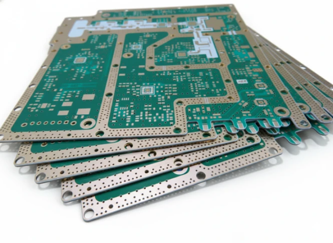
Integrating Radio Frequency (RF) components into compact System-in-Package (SiP) modules is no longer optional for modern 5G and aerospace applications; it is a necessity. Overmolding for RF front-end—the process of encapsulating RF circuits with a protective compound—offers superior durability and form factor reduction. However, it introduces significant complexity. The molding compound is not electrically invisible; it interacts with electromagnetic fields, potentially detuning antennas, shifting impedance, and degrading signal integrity.
This playbook is designed for RF Engineers, Product Architects, and Procurement Leads who need to transition a design from a bare-die or open-frame prototype to a fully encapsulated, mass-producible module. We move beyond basic definitions to provide a decision-making framework. You will find specific technical requirements to define in your documentation, a breakdown of hidden risks that cause yield loss, and a rigorous validation plan to ensure the final product performs as simulated.
At APTPCB (APTPCB PCB Factory), we see many designs fail not because of poor circuit theory, but because the physical interaction between the molding compound and the RF layout was underestimated. This guide helps you anticipate those physical realities. It provides the checklists needed to audit suppliers and the trade-off logic required to make safe engineering decisions.
When overmolding for RF front-end is the right approach (and when it isn’t)
Before committing to the tooling costs of overmolding, it is critical to verify that this packaging method aligns with your product goals. Overmolding is not a universal solution for all RF applications.
It is the Right Approach When:
- Miniaturization is Critical: You need to reduce the Z-height and XY footprint significantly compared to metal can shielding.
- Environmental Protection is Mandatory: The device operates in high-humidity, vibration-prone, or corrosive environments (e.g., automotive radar, aerospace sensors).
- High-Volume Manufacturing: You are scaling to volumes where the unit cost of molding is lower than the assembly cost of mechanical lids and screws.
- System-in-Package (SiP) Integration: You are combining heterogeneous dies (GaAs, GaN, CMOS) and passives into a single module that needs to handle like a standard SMT component.
It is the Wrong Approach When:
- Prototyping or Low Volume: The NRE (Non-Recurring Engineering) costs for mold chases and flow analysis are prohibitive for runs under 5,000 units.
- Ultra-High Power RF: If the thermal dissipation requirements exceed the thermal conductivity of the molding compound, the device will overheat. Air cavities or open-frame designs are better for extreme heat flux.
- Post-Production Tuning is Required: Once molded, the circuit is inaccessible. If your design relies on manual antenna tuning and trimming on the production line, overmolding will block access to the tuning elements.
- Extreme Sensitivity to Dielectric Loading: If the circuit cannot tolerate the dielectric shift caused by the mold compound (and cannot be compensated for in design), an air-cavity package is safer.
Specs & requirements (before quoting)
To get an accurate quote and a viable manufacturing process, you must provide more than just a Gerber file. The interaction between the overmolding for RF front-end process and the electrical performance requires a detailed specification sheet.
Material and Stackup Specifications:
- Mold Compound Dk/Df: Specify the target Dielectric Constant ($D_k$) and Dissipation Factor ($D_f$) at your operating frequency (e.g., 28GHz or 77GHz). Do not accept "standard epoxy" without data.
- Filler Particle Size: Define maximum filler size (e.g., < 25 microns) to ensure flow into tight gaps between 01005 passives or under flip-chips.
- CTE Mismatch: Specify the acceptable Coefficient of Thermal Expansion (CTE) range to match your PCB substrate, minimizing warpage.
- Glass Transition Temperature (Tg): Define a Tg that exceeds your maximum reflow and operating temperatures (typically > 150°C or > 175°C for high-reliability).
Mechanical and Tolerance Targets:
- Mold Cap Height Tolerance: $\pm$ 25 microns or tighter, depending on the application’s Z-height constraints.
- Wire Loop Height Clearance: Minimum clearance between the top of the wire bond loop and the top of the mold cap (typically > 50 microns) to prevent wire exposure.
- Keep-Out Zones: Clearly defined areas on the PCB where mold compound must not flow (e.g., connector pads, thermal pads).
- Warpage Limits: Maximum allowable bow/twist across the module (e.g., < 0.08mm) to ensure successful SMT assembly later.
RF Performance Requirements:
- Frequency Shift Tolerance: Maximum allowable center frequency shift post-mold (e.g., $\pm$ 50 MHz).
- Insertion Loss Delta: Maximum acceptable increase in insertion loss due to the molding compound (e.g., < 0.5 dB).
- Return Loss Minimum: The minimum return loss required after the dielectric loading of the mold is applied.
Process and Reliability:
- Void Criteria: Maximum allowable void size and percentage (e.g., no voids > 10 microns in active RF areas).
- Moisture Sensitivity Level (MSL): Target MSL rating (usually MSL 3 or better).
- mmWave Module SMT Process Compatibility: The molded module must survive secondary reflow cycles without delamination or popcorning.
Hidden risks (root causes & prevention)
Scaling overmolding for RF front-end reveals physics-based risks that do not appear in software simulations. Understanding these failure modes allows you to detect them during the NPI (New Product Introduction) phase.
1. Dielectric Detuning (The "Frequency Shift")
- Risk: The molding compound has a $D_k$ of 3.0–4.0, whereas air is 1.0. This adds capacitance to every exposed conductor.
- Why it happens: The electromagnetic fields fringe into the mold compound, slowing the wave velocity and shifting resonance to lower frequencies.
- Detection: Compare S-parameters of bare boards vs. molded boards.
- Prevention: Pre-distort the design (design for a higher frequency) so the mold shift lands it on target. Use electromagnetic simulation with accurate material properties.
2. Wire Bond Sweep
- Risk: The high-pressure flow of the molding compound pushes wire bonds, causing them to touch (short) or change shape.
- Why it happens: Viscosity of the compound is too high, or injection speed is too fast.
- Detection: X-ray inspection post-mold; erratic inductance values in RF testing.
- Prevention: Use "Low Sweep" molding compounds with lower viscosity. Optimize wire bond profiles (lower loops, shorter lengths).
3. CTE Mismatch and Warpage
- Risk: The PCB, the silicon die, and the mold compound expand at different rates. Upon cooling, the module warps.
- Why it happens: Poor selection of mold compound CTE relative to the substrate.
- Detection: Shadow Moiré measurement; coplanarity failures during SMT.
- Prevention: Select a mold compound with a CTE closely matched to the PCB substrate (e.g., organic substrate vs. ceramic).
4. Incomplete Filling (Short Shots) and Voids
- Risk: Air pockets trapped under components or between wires.
- Why it happens: Air cannot escape fast enough during injection, or filler particles clog narrow gaps.
- Detection: Scanning Acoustic Microscopy (CSAM) or X-ray.
- Prevention: Vacuum-assisted molding (VAM); optimizing gate location and vent design; selecting appropriate filler particle sizes.
5. Delamination at Interfaces
- Risk: The mold compound separates from the PCB surface or the die surface.
- Why it happens: Surface contamination (flux residue), moisture expansion (popcorning), or poor adhesion chemistry.
- Detection: CSAM; electrical failure after thermal cycling.
- Prevention: Plasma cleaning prior to molding to activate surfaces; strict moisture control (baking) before molding.
6. EMI Shielding Inconsistency
- Risk: If using conformal shielding (sputtering over the mold), surface defects on the mold cause gaps in the shield.
- Why it happens: Pits, voids, or contamination on the exterior of the mold cap.
- Detection: Visual inspection; radiated emissions testing.
- Prevention: High-quality mold release agents; precise mold tool surface finish.
7. Thermal Trapping
- Risk: The mold compound acts as a thermal blanket, trapping heat in the PA (Power Amplifier).
- Why it happens: Epoxy is generally a poor thermal conductor compared to air convection or metal lids.
- Detection: Thermal imaging (if possible) or junction temperature monitoring.
- Prevention: Use thermally conductive mold compounds; design thermal vias and exposed pads on the bottom of the PCB.
8. Stress-Induced Piezoelectric Effects
- Risk: Mechanical stress from the mold alters the performance of sensitive components like MLCCs or MEMS.
- Why it happens: Compressive stress from curing shrinkage.
- Detection: Shift in capacitance values or filter characteristics.
- Prevention: Use low-stress (low modulus) molding compounds; orient sensitive components to minimize stress impact.
Validation plan (what to test, when, and what “pass” means)
A robust validation plan for overmolding for RF front-end must correlate physical integrity with RF performance. You cannot rely on electrical testing alone.
1. Visual and X-Ray Inspection (Post-Mold, Pre-Cure)
- Objective: Detect gross defects immediately.
- Method: High-resolution X-ray (2D/3D).
- Acceptance: No wire sweep > 5% of wire length; no visible voids > 50 microns in critical areas.
2. Scanning Acoustic Microscopy (CSAM)
- Objective: Detect internal delamination and voids that X-ray misses.
- Method: C-Mode scanning of the interface between mold/die and mold/substrate.
- Acceptance: < 5% delamination area; zero delamination on wire bond pads or active RF paths.
3. Cross-Sectioning (Destructive)
- Objective: Verify vertical fill and wire loop clearance.
- Method: Mechanical cross-section and SEM analysis.
- Acceptance: No voids under flip-chips; wire loop clearance > 50 microns from top of mold.
4. RF Bench Testing (S-Parameters)
- Objective: Quantify the dielectric shift.
- Method: Vector Network Analyzer (VNA) measurement of gain, return loss, and isolation.
- Acceptance: Center frequency shift within design margin (e.g., < 2%); Insertion loss degradation < 0.5dB.
5. Thermal Cycling (Reliability)
- Objective: Stress the CTE mismatch interfaces.
- Method: -40°C to +125°C (or +150°C), 500 to 1000 cycles.
- Acceptance: No electrical open/shorts; no delamination growth in CSAM post-test.
6. High Temperature Operating Life (HTOL)
- Objective: Verify long-term stability under power and heat.
- Method: Continuous operation at max rated temperature for 1000 hours.
- Acceptance: RF performance remains within spec; no thermal runaway.
7. Moisture Sensitivity Level (MSL) Testing
- Objective: Verify resistance to moisture-induced cracking during reflow.
- Method: Soak at defined humidity/temp, followed by 3x reflow simulation.
- Acceptance: No popcorning; no internal delamination; electrical pass.
8. Drop Testing
- Objective: Verify mechanical adhesion under shock.
- Method: Standard JEDEC drop test.
- Acceptance: No package cracking; no solder joint fractures (if module is mounted).
9. Warpage Measurement
- Objective: Ensure SMT compatibility.
- Method: Shadow Moiré at room temp and reflow temp (260°C).
- Acceptance: Warpage < 0.08mm (or specific coplanarity spec).
10. Chemical Resistance (Optional)
- Objective: Ensure mold withstands cleaning agents.
- Method: Immersion in standard flux cleaners.
- Acceptance: No surface degradation or swelling.
Supplier checklist (RFQ + audit questions)
When selecting a partner for overmolding for RF front-end, general PCB assembly capabilities are insufficient. You need a supplier with specific packaging expertise. Use this checklist to vet APTPCB or any other vendor.
Group 1: RFQ Inputs (What you must provide)
- Gerber & ODB++ Files: Complete layout data.
- 3D STEP File: Critical for mold tool design, showing component heights.
- Bill of Materials (BOM): Including specific part numbers for all passives and dies.
- Panel Drawing: Preferred panel utilization and fiducial locations.
- RF Specs: Target frequency, max loss, and dielectric constant requirements.
- Volume Forecast: EAU (Estimated Annual Usage) to determine tooling class (soft tool vs. hard tool).
- Testing Requirements: List of RF tests required on the production line.
- Packaging Requirements: Tape & Reel specs for the finished module.
Group 2: Capability Proof (What to ask the supplier)
- Mold Flow Analysis: Can they simulate the injection process to predict voids and wire sweep before cutting steel?
- Material Library: Do they have experience with low-loss, low-CTE molding compounds (e.g., Sumitomo, Hitachi)?
- RF Competence: Do they understand $D_k$/$D_f$ implications, or are they just a mechanical molding house?
- Equipment Precision: What is the tolerance of their molding chase? (Should be micron-level).
- Vacuum Molding: Do they have vacuum-assisted systems to eliminate voids in dense RF clusters?
- Post-Mold Curing: Do they have programmable ovens with precise ramp profiles?
Group 3: Quality System & Traceability
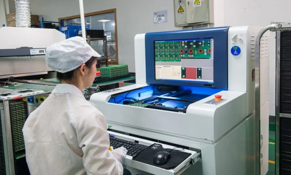
- X-Ray Capacity: Is X-ray 100% or sampling? What is the resolution?
- CSAM Availability: Do they have in-house CSAM for delamination checks?
- Wire Bond Inspection: Automated Optical Inspection (AOI) for wire bonds pre-mold?
- Plasma Cleaning: Is plasma cleaning standard in their process flow before molding?
- Traceability: Can they trace a specific module back to the mold shot and compound batch?
- Clean Room Class: Is the molding area in a controlled clean room environment (Class 10k or better)?
Group 4: Change Control & Delivery
- PCN Policy: Will they notify you if they change the mold compound formulation? (Critical for RF).
- Tool Maintenance: What is the cleaning and maintenance schedule for the mold chases?
- Yield Management: How do they handle bad units in a panel? (Marking vs. punching out).
- Capacity Planning: Can they scale from NPI to mass production without changing equipment sets?
- Lead Time: What is the lead time for new mold tooling vs. repeat production?
Decision guidance (trade-offs you can actually choose)
Engineering is about compromise. In overmolding for RF front-end, you cannot maximize every parameter simultaneously. Here are the realistic trade-offs.
1. Performance vs. Protection
- If you prioritize maximum RF efficiency: Choose an air-cavity package or conformal coating.
- If you prioritize environmental robustness and size: Choose overmolding.
- Trade-off: You sacrifice some RF signal integrity (due to dielectric loss) for superior physical protection.
2. Thermal vs. Electrical Isolation
- If you prioritize thermal dissipation: Choose a compound with high thermal conductivity (ceramic fillers).
- If you prioritize electrical isolation: Choose a standard epoxy.
- Trade-off: Thermally conductive compounds are often more abrasive to mold tools and may have higher $D_k$, affecting RF tuning.
3. Cost vs. Development Speed
- If you prioritize speed: Use "soft tooling" or machined aluminum molds.
- If you prioritize unit cost: Invest in hardened steel multi-cavity molds.
- Trade-off: Soft tools wear out fast and have looser tolerances but are cheap and quick to make. Hard tools are expensive and slow to build but yield millions of consistent parts.
4. Integration vs. Yield
- If you prioritize density: Put everything (PA, LNA, Switch, Filter) in one mold.
- If you prioritize yield: Split the system into smaller sub-modules.
- Trade-off: A "mega-module" saves space but if one die fails, the whole module is scrapped. Smaller modules have higher assembly overhead but lower scrap costs.
5. Standard vs. Custom Material
- If you prioritize supply chain security: Use industry-standard molding compounds.
- If you prioritize RF performance: Use specialized low-loss compounds.
- Trade-off: Specialized materials have longer lead times, higher MOQs, and fewer alternative suppliers.
FAQ
Q: Can we rework an overmolded RF module? A: No. Once the thermoset epoxy cures, it cannot be removed without destroying the components. Rework must happen pre-mold.
Q: How accurate are RF simulations with mold compound? A: Accuracy depends on the material data. If you use generic datasheet values for $D_k$, simulation will be off. You must use frequency-dependent data provided by the material vendor or measured characterization.
Q: Does overmolding affect EMI shielding? A: Yes, the mold itself is not a shield. However, overmolding creates a smooth surface that is ideal for applying a sputtered metal conformal shield (sputtering) directly on the package, which is highly effective.
Q: What is the typical thickness of the mold cap? A: It varies, but typically ranges from 0.3mm to 1.0mm above the PCB surface, depending on the tallest component and required wire loop clearance.
Q: Can we use overmolding for mmWave (28GHz+)? A: Yes, but material selection is critical. Standard epoxies are too lossy. You need specialized low-loss compounds designed for mmWave to minimize signal attenuation.
Q: How does overmolding impact the mmWave module SMT process?
A: The module becomes a robust component. However, you must ensure the moisture is baked out before SMT reflow to prevent "popcorning" (explosive delamination due to steam pressure).
Q: Is antenna tuning and trimming possible after molding?
A: Generally, no. Laser trimming requires line-of-sight. All tuning must be dynamic (electronic) or the design must be robust enough to tolerate the mold shift without physical trimming.
Q: What is the cost difference between overmolding and metal cans? A: At low volumes, metal cans are cheaper (no tooling). At high volumes (>100k units), overmolding is significantly cheaper per unit and uses less PCB real estate.
Related pages & tools
- Microwave PCB Manufacturing: Understanding the base substrate is the first step before considering the mold compound that goes on top of it.
- NPI & Small Batch Assembly: Learn how to validate your RF design in small batches before committing to expensive hard mold tooling.
- X-Ray Inspection Services: A critical validation step for detecting wire sweep and voids inside the molded package.
- Turnkey PCB Assembly: Explore how APTPCB handles the entire flow from PCB fabrication to component sourcing and final molding.
- Rogers PCB Materials: High-frequency laminates are often required for the substrate of overmolded RF modules to maintain signal integrity.
Request a quote
Ready to move your RF design from concept to a fully encapsulated module? APTPCB offers comprehensive DFM reviews to catch molding risks before you cut steel.
For a precise quote and DFM, please prepare:
- Gerber Files (for the substrate).
- 3D STEP File (for mold cap design).
- BOM (with specific component heights).
- RF Requirements (Frequency, Max Loss).
- Volume Estimates (to determine tooling strategy).
Click here to Request a Quote & DFM Review – Our engineering team will review your stackup and mold requirements to ensure a successful scale-up.
Conclusion
Overmolding for RF front-end is a transformative packaging technology that enables the density required for 5G and future wireless systems. However, it is not merely a mechanical housing; it is an integral part of the RF circuit that alters impedance, thermal performance, and reliability. By defining strict material requirements, anticipating risks like wire sweep and dielectric detuning, and enforcing a rigorous validation plan, you can leverage the benefits of overmolding without sacrificing signal integrity. Success lies in treating the mold compound as a critical RF component, not just a protective shell.