Contents
- Highlights
- PCB Cost Reduction: Definition and Scope
- PCB Cost Reduction Rules and Specifications
- PCB Cost Reduction Implementation Steps
- PCB Cost Reduction Troubleshooting
- 6 Essential Rules for PCB Cost Reduction (Cheat Sheet)
- FAQ
- Request a Quote / DFM Review for PCB Cost Reduction
- Conclusion
In the world of electronics manufacturing, pcb cost reduction is not merely about selecting the cheapest laminate or cutting corners on quality; it is a disciplined engineering process of optimizing Design for Manufacturing (DFM). As CAM engineers at APTPCB, we see thousands of designs where simple over-specifications—such as unnecessary blind vias, non-standard stackups, or inefficient panel utilization—inflate production costs by 30% to 50% without adding performance value. True cost reduction is achieved by aligning your design parameters with standard manufacturing capabilities to maximize yield and throughput.
Quick Answer
To achieve effective pcb cost reduction, you must focus on standardizing materials and relaxing tolerances to "standard" manufacturing tiers rather than "advanced" tiers wherever possible.
- Maximize Panel Utilization: Aim for ≥80% usage of the working panel. Poor utilization means you are paying for waste material.
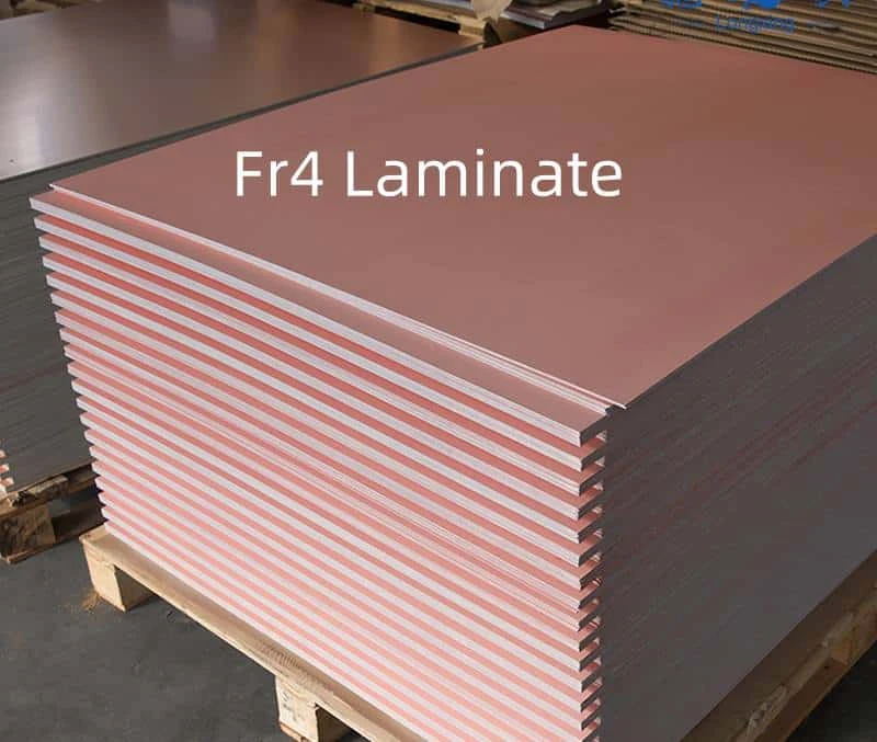
- Stick to Standard Materials: Use standard FR4 (TG150) unless high-speed or high-temp requirements strictly dictate otherwise.
- Minimize Layer Count: Every pair of layers adds lamination cycles and material cost. Compress designs where signal integrity allows.
- Optimize Via Tech: Avoid blind and buried vias (HDI) if through-holes can suffice. HDI adds sequential lamination steps that drastically increase price.
- Standardize Trace/Space: Keep trace width and spacing ≥ 5mil (0.127mm). Going below 4mil often requires specialized etching and inspection, raising costs.
- Verification: Always run a DFM check using tools like a Gerber Viewer to identify "advanced" features that trigger price premiums.
Highlights
- Material Selection: The substrate accounts for 30-40% of the board cost; switching from specialized RF materials to standard FR4 where possible yields immediate savings.
- Drill Efficiency: Reducing the number of drill hits and increasing the minimum hole size (>0.3mm) extends drill bit life and reduces machine time.
- Surface Finish: ENIG is excellent for flatness, but HASL or OSP are significantly cheaper for general-purpose boards.
- Volume Batching: Ordering in standard production lot sizes (e.g., 5m² or 10m²) amortizes setup costs more effectively than small prototype runs.
PCB Cost Reduction: Definition and Scope
At its core, pcb cost reduction is the strategic management of four main cost drivers: Laminate (Material), Manufacturing Process (Labor/Machine Time), Yield (Scrap Rate), and Overhead (Setup/Testing).
Many designers focus solely on the unit price of the bare board, ignoring how design decisions impact the PCB fabrication process. For instance, specifying a tight tolerance of ±5% on controlled impedance might force the manufacturer to use higher-grade materials and perform 100% coupon testing, whereas a standard ±10% tolerance allows for standard processing. Similarly, the choice of panelization affects not just the PCB cost but the assembly efficiency; a panel with too many "X-outs" (bad boards) slows down the SMT line.
The goal is to design a board that fits comfortably within the "sweet spot" of your manufacturer's capabilities. When a design pushes the limits (e.g., aspect ratios > 8:1, 3mil traces), yields drop, and the manufacturer must price in the expected scrap.

Tech / Decision Matrix
The following matrix outlines specific design levers and their direct impact on manufacturing complexity and cost.
Tech / Decision Lever → Practical Impact
| Decision Lever / Spec | Practical Impact (Yield/Cost/Reliability) |
|---|---|
| Via Technology (Through vs. HDI) | High Impact. Through-hole vias are drilled in one pass. Blind/Buried vias require sequential lamination and laser drilling, often increasing cost by 40-60%. |
| Panel Utilization | Medium-High Impact. Manufacturers use standard sheet sizes (e.g., 18"x24"). If your array fits poorly (e.g., 60% usage), you pay for the 40% scrap. |
| Minimum Hole Size | Medium Impact. Holes < 0.2mm require expensive CNC machines or lasers and limit stack height (drilling fewer boards at once). Keep holes ≥ 0.3mm for standard pricing. |
| Surface Finish | Medium Impact. Hard Gold is expensive due to material cost. ENIG is standard but pricier than HASL or OSP. Use OSP for cost-sensitive consumer electronics. |
| Copper Weight | Low-Medium Impact. 1oz is standard. 2oz or 3oz increases etching time and requires wider spacing (clearance), reducing density and potentially forcing more layers. |
PCB Cost Reduction Rules and Specifications
To systematically drive down costs, engineers should adhere to "Standard" fabrication specifications. Deviating into "Advanced" or "Cutting Edge" tiers triggers price multipliers. Below are the recommended specifications for a cost-optimized FR4 PCB.
| Rule | Recommended Value | Why it matters | How to verify |
|---|---|---|---|
| Trace / Space | ≥ 5mil / 5mil (0.127mm) | Tighter spacing lowers yield due to potential shorts/opens during etching. | Run DRC (Design Rule Check) in CAD software. |
| Min Drill Size | ≥ 0.3mm (12mil) | Smaller drills break easily, require slower speeds, and limit stack height. | Check drill table in Gerber files. |
| Annular Ring | ≥ 5mil (0.127mm) | Ensures the drill hits the pad even with mechanical tolerance. Prevents breakout. | Visual inspection of pad vs. hole size. |
| Board Shape | Rectangular | Complex shapes require longer routing time and generate more waste. | Review board outline layer. |
| Solder Mask | Green | Green is produced in massive bulk and cures fastest. Other colors (Blue, Red, Black) often have setup fees. | Specify "Green LPI" in fabrication notes. |
| Layer Count | Even Numbers (2, 4, 6) | Odd layer counts (e.g., 3, 5) require non-standard lamination and often warp, leading to scrap. | Check stackup configuration. |
Material Standardization
Using exotic materials is the fastest way to blow a budget. For 90% of applications, standard FR4 (Tg150 or Tg170) is sufficient. If you specify a specific brand (e.g., "Isola 370HR only"), the factory may have to order it specifically for you, adding lead time and cost. Instead, specify "IPC-4101/126 or equivalent" to allow the factory to use their stocked inventory.

PCB Cost Reduction Implementation Steps
Implementing cost reduction is a workflow that begins at the schematic stage and continues through procurement.
Implementation Process
Step-by-step execution guide
Before routing traces, set up your CAD constraints to match the "Standard" capabilities of your vendor. Don't default to 3mil/3mil just because the software allows it. Consult the manufacturer's capability sheet first.
Work with your CAM engineer to design the delivery array. Sometimes rotating a board 90 degrees or adding/removing a unit from the array can increase material utilization from 60% to 85%, directly reducing unit cost.
For PCBA, consolidate [component sourcing](/en/pcba/component-sourcing). Reduce unique part numbers (e.g., use 10kΩ resistors everywhere possible). This reduces feeder setup time on the pick-and-place machine.
Review the fabrication notes. Do you really need IPC Class 3 for a consumer toy? Do you need plugged vias? Removing unnecessary requirements prevents the factory from adding risk premiums to the quote.
PCB Cost Reduction Troubleshooting
Even with good intentions, cost reduction efforts can backfire if not executed carefully. Here are common pitfalls and how to fix them.
1. The "False Economy" of Layer Reduction
Problem: A designer aggressively reduces a 6-layer board to 4 layers to save 15% on laminate. Failure Mode: To fit the routing on fewer layers, trace spacing is reduced to 3mil, and via sizes are shrunk to 0.15mm. Result: The board moves from "Standard" to "Advanced" technology. The yield drops, and the price actually increases by 20% due to the tighter tolerances. Fix: Balance layer count with density. Sometimes a 6-layer board with loose tolerances is cheaper than a 4-layer board with tight tolerances.
2. Cheap Material Warpage
Problem: Specifying the absolute cheapest generic FR4 for a lead-free assembly. Failure Mode: Lead-free reflow temperatures (260°C) cause the low-Tg material to delaminate or warp significantly. Result: High scrap rates during assembly. Fix: Ensure the material Tg (Glass Transition Temperature) matches the assembly profile. Tg150 is the safe baseline for most lead-free processes.
3. Over-Panelization
Problem: Putting too many small boards on a large panel to "save handling time." Failure Mode: The large panel becomes flimsy and sags during wave soldering or reflow, causing defects. Result: Need for expensive custom fixtures or pallets. Fix: Keep panel sizes manageable (e.g., max 200mm x 300mm for thin boards) or add breakaway tabs for rigidity.

6 Essential Rules for PCB Cost Reduction (Cheat Sheet)
| Rule / Guideline | Why It Matters (Physics/Cost) | Target Value / Action |
|---|---|---|
| Standardize Vias | Microvias and blind vias require laser drilling and extra plating cycles. | Through-hole only (Min 0.3mm) |
| Relax Tolerances | Tight tolerances (e.g., ±5% impedance) force 100% testing and lower yield. | Standard ±10% or ±20% |
| Optimize Panel | Unused laminate on the production panel is paid waste. | >80% Utilization |
| Surface Finish | Gold is expensive; HASL is robust and cheap. | HASL (Lead-Free) or OSP |
| Copper Weight | Heavy copper requires more etching time and wider spacing. | 1 oz (35µm) |
| Solder Mask | Green cures faster and is the industry standard volume runner. | Green LPI |
FAQ
Q: Does Reducing the PCB Size Always Reduce the Cost?
A: Not always. While less material is used, if the size reduction forces you to increase layer count (e.g., 4 to 6 layers) or use HDI technology to fit the components, the cost will likely increase. Additionally, if the board becomes too small to handle effectively, assembly costs may rise due to fixturing requirements.
Q: Is OSP Cheaper Than ENIG?
A: Yes, OSP (Organic Solderability Preservative) is generally cheaper than ENIG (Electroless Nickel Immersion Gold). OSP is a simple water-based chemical process, whereas ENIG involves expensive gold salts and complex chemical monitoring. However, ENIG offers better shelf life and planarity for fine-pitch components.
Q: How Does Lead Time Affect PCB Cost?
A: Lead time is a major cost factor. "Quick Turn" services (24-48 hours) disrupt standard production flows and require dedicated machine time, attracting a premium of 50% to 200%. Planning ahead for a standard lead time (e.g., 5-7 days) is the easiest way to secure pcb cost reduction.
Q: Can I Save Money by Skipping Electrical Testing?
A: We strongly advise against this. While it saves a small amount upfront, the cost of finding a short circuit after components are assembled (or worse, in the field) is exponentially higher. Electrical testing (E-Test) is a standard quality gate at APTPCB. ---
Request a Quote / DFM Review for PCB Cost Reduction
Ready to optimize your design for mass production? Send us your data for a free DFM and cost analysis. Please include:
- Gerber Files: RS-274X format preferred.
- Fabrication Drawing: Specifying material, thickness, and finish.
- Quantity: Prototype vs. Production volumes (e.g., 50 vs 5000 pcs).
- Special Requirements: Impedance control, specific stackup, etc.
Conclusion
Achieving sustainable pcb cost reduction requires a holistic view of the manufacturing process. It is about making informed trade-offs—choosing standard materials, optimizing panel usage, and designing within standard process windows. By engaging with your manufacturer early in the design phase, you can identify cost drivers before they are locked in.
At APTPCB, our engineering team is dedicated to helping you navigate these decisions to deliver high-quality boards at the most competitive prices.
Signed, The Engineering Team at APTPCB