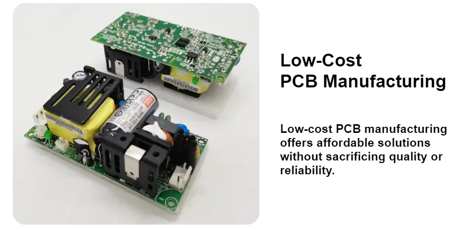
Optimizing printed circuit board (PCB) fabrication costs requires a delicate balance between electrical performance, mechanical constraints, and manufacturing capabilities. Many engineers inadvertently inflate production costs by specifying tighter tolerances or more complex features than necessary, often unaware of the specific cost drivers in the fabrication process. By understanding the relationship between design decisions and factory floor operations, you can achieve significant savings while maintaining high reliability.
Highlights
- Material Utilization: Learn how panel efficiency impacts unit price and how to design for standard working panel sizes.
- Layer Count Strategy: Methods to reduce layer counts through smarter routing and component placement.
- Via Technology: The cost implications of blind, buried, and microvias versus standard through-hole technology.
- Surface Finishes: A comparative analysis of HASL, ENIG, and OSP regarding cost versus shelf life and planarity.
- Tolerances: How relaxing non-critical mechanical and electrical tolerances can reduce scrap rates and lower quotes.
Contents
- 1. Material Selection and Panel Utilization
- 2. Layer Count and Stack-up Optimization
- 3. Via Technology and Drilling Constraints
- 4. Trace, Space, and Copper Weight
- 5. Surface Finishes: Balancing Cost and Performance
- 6. How to Estimate PCB Cost from Gerber Files
- 7. Quantity and Lead Time Strategies
- 8. Testing and Inspection Protocols
- 9. Advanced Design for Manufacturability (DFM)
- 10. Sourcing and Vendor Selection
- Summary Checklist for Cost Reduction
1. Material Selection and Panel Utilization
The raw laminate constitutes a significant portion of the total board cost, especially for multilayer PCBs. Choosing the right material and ensuring it fits efficiently on the manufacturer's production panel is the first step in low cost PCB manufacturing.
The Rule of Standard Materials
Rule: Stick to standard FR4 (TG130-150) unless the application strictly demands high-speed or high-temperature performance. Why it Matters: Standard FR4 is produced in massive volumes, keeping costs low. Specialty materials like Rogers or high-TG FR4 (TG170+) can cost 2x to 10x more per sheet. How to Verify: Check your datasheet. If your operating temperature is under 100°C and signal frequencies are below 1-2 GHz, standard FR4 is likely sufficient. Common Pitfall: Specifying TG180 "just to be safe" for a consumer device operating at room temperature.
Panel Utilization Efficiency
PCB manufacturers do not fabricate boards one by one; they process large working panels (typically 18"x24", 21"x24", or larger). The percentage of that panel covered by your usable PCBs determines your material waste.
- Target Range: Aim for >80% panel utilization.
- The Math: If your board is 50mm x 50mm, and the working panel allows a 5mm clearance, fitting an array that utilizes only 60% of the panel means you are paying for 40% scrap.
- Action: Consult your manufacturer early about their preferred working panel sizes. Sometimes changing a dimension by just 1-2mm can allow an extra row or column of boards on the panel, reducing the unit cost by 15-20%.
For more on material properties, explore our guide on FR4 PCB options.
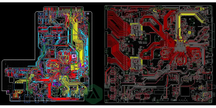
2. Layer Count and Stack-up Optimization
Reducing the layer count is one of the most direct ways to lower costs, but it must be done without compromising signal integrity.
The Cost of Lamination
Each additional pair of layers adds a lamination cycle, more prepreg material, and increased processing time.
- Jump Costs: Moving from 2 layers to 4 layers typically increases cost by 30-40%. Moving from 4 to 6 layers adds another 20-30%.
- Standard Stacks: Stick to even layer counts (2, 4, 6, 8). Odd layer counts (e.g., 5 layers) usually require a non-standard lamination process that can warp the board and actually cost more than a 6-layer board due to the need for special handling.
Routing Efficiency
Rule: Exhaust all routing possibilities on outer layers before adding inner layers. Why it Matters: Engineers often jump to a 6-layer stack for convenience. How to Verify: Use autorouters only for estimation; manual routing often reveals that a 4-layer stack is viable if component placement is optimized. Common Pitfall: Using a 6-layer stack solely for power planes when a poured copper polygon on a signal layer would suffice.
Review our PCB Stack-up guidelines to understand standard dielectric thicknesses.
3. Via Technology and Drilling Constraints
Drilling is the slowest and most expensive mechanical process in PCB fabrication. The number of holes, their size, and the technology used (mechanical vs. laser) drive costs significantly.
Drill Size and Aspect Ratio
Rule: Keep minimum mechanical drill sizes ≥ 0.2mm (8 mil) and aspect ratios < 8:1. Why it Matters:
- Drill Wear: Smaller bits break more often and have shorter lifespans.
- Stacking: Manufacturers can stack 2-3 panels to drill simultaneously if holes are >0.3mm. For holes <0.2mm, they must drill panels individually, tripling the machine time.
- Aspect Ratio: The ratio of board thickness to hole diameter. If a board is 1.6mm thick and the hole is 0.2mm, the ratio is 8:1. Ratios above 10:1 make plating difficult, requiring advanced chemical processes that increase cost.
Hdi and Advanced Vias
High Density Interconnect (HDI) features like blind and buried vias require sequential lamination.
- Cost Impact: Adding blind vias can increase board cost by 50-80% compared to a standard through-hole board.
- Alternative: Before committing to HDI PCB technology, try reducing component density or increasing board size slightly to allow for standard through-hole routing.
Hole Count
Rule: Minimize the total number of holes. Threshold: Many manufacturers have a threshold (e.g., 50 holes per square inch or 100,000 holes per batch) where surcharges apply due to excessive drill wear and machine time.
4. Trace, Space, and Copper Weight
Pushing the limits of etching capabilities reduces yield. Lower yield means the manufacturer must produce more panels to ensure enough good boards pass inspection, and this cost is passed to you.
Trace/space Tolerances
- Standard: 5/5 mil (0.127mm) or 6/6 mil (0.152mm). This is the "safe zone" for most fabs.
- Advanced: 3/3 mil (0.076mm) or 4/4 mil.
- Cost Driver: Going below 4/4 mil often requires stricter cleanroom controls and slower etching speeds. It can increase the base price by 20-30%.
Copper Weight
Rule: Use 1oz (35µm) copper unless high current demands 2oz or more. Why it Matters: Heavier copper requires wider spacing between traces to etch cleanly.
- Constraint: For 1oz copper, min space is typically 4-5 mil. For 2oz copper, min space jumps to 8-10 mil.
- Pitfall: Specifying 2oz copper on all layers when only the power layer needs it. If you need high current, consider Heavy Copper PCB solutions only where necessary or use busbars.
5. Surface Finishes: Balancing Cost and Performance
The surface finish protects the copper from oxidation and ensures solderability.
| Finish | Cost | Shelf Life | Planarity | Best For |
|---|---|---|---|---|
| HASL (Leaded) | Lowest | 12 Months | Poor | Through-hole, simple SMT |
| HASL (Lead-Free) | Low | 12 Months | Poor | RoHS compliance, general use |
| OSP | Low | 6 Months | Excellent | Fine-pitch SMT, controlled storage |
| ENIG | Medium/High | 12+ Months | Excellent | BGAs, wire bonding, touch contacts |
| Hard Gold | Highest | Years | Excellent | Edge connectors, wear resistance |
Recommendation: Use Lead-Free HASL for general electronics. Upgrade to ENIG only if you have fine-pitch components (BGA, QFN) or require a perfectly flat surface. Avoid Hard Gold unless you have edge connectors that will be inserted/removed repeatedly.
6. How to Estimate PCB Cost from Gerber Files
Understanding how to estimate PCB cost from Gerber data allows you to audit your designs before quoting. When a CAM engineer reviews your files, they look for "cost adders."
The "Cost Adder" Checklist
- Slot Milling: Are there plated slots? These require a secondary drilling/routing step.
- Castellated Holes: Half-cut holes on the edge require specialized routing and handling.
- Small Annular Rings: If the pad size minus the drill size is < 4 mil, it requires high-precision alignment (Registration), increasing cost.
- Peelable Mask: Used to protect holes during wave soldering. This is a manual application process.
- Via Filling: Conductive or non-conductive via filling (POFV) is significantly more expensive than simple tenting with solder mask.
Self-Check: Run your Gerbers through a DFM tool or a Gerber Viewer to identify these features. If a feature isn't critical, remove it.
7. Quantity and Lead Time Strategies
The economics of PCB manufacturing are heavily driven by setup costs and economies of scale.
The Setup Fee Trap
Every order incurs NRE (Non-Recurring Engineering) costs: CAM review, film generation, stencil creation, and machine setup.
- Scenario: Ordering 5 prototypes might cost $100 ($20/board). Ordering 50 might cost $200 ($4/board).
- Strategy: If you are confident in the design, ordering a slightly larger pilot run (e.g., 50 units) is often more cost-effective per unit than ordering 5, then 10, then 20.
Lead Time
Rule: Plan ahead to avoid "Quick Turn" premiums. Range: A standard lead time is 5-7 days. Requesting a 24-hour or 48-hour turn can increase the price by 100% to 200%. Logistics: Consolidate orders. Shipping 5 different PCB designs in one package saves significantly on international freight.
8. Testing and Inspection Protocols
Quality assurance is vital, but over-specifying test requirements adds unnecessary expense.
Electrical Testing (E-Test)
- Flying Probe: Good for prototypes and small volumes. No fixture cost, but slow per board.
- Bed of Nails (Fixture): High setup cost ($200-$500+), but very fast per board.
- Decision: For orders under 50 sq. meters or small batches, flying probe is standard and usually included in the price. Do not request fixture testing for prototypes.
IPC Class Requirements
- IPC Class 2: Standard for most industrial and consumer electronics.
- IPC Class 3: Required for aerospace, medical, and life-support systems.
- Cost: Class 3 requires tighter annular rings, more plating thickness in holes, and stricter inspection criteria, often raising costs by 20-40%.
- Verify: Does your LED controller really need Class 3 reliability? Likely not.
9. Advanced Design for Manufacturability (DFM)
Implementing robust DFM Guidelines is the ultimate cost reduction tool. It prevents the "on-hold" status where engineering questions (EQs) delay production and potentially force costly redesigns.
Solder Mask Dams
Rule: Maintain a minimum solder mask dam of 4 mil (0.1mm) between pads. Failure: If the dam is too small, the manufacturer must gang-relieve the mask (remove it entirely between pads), increasing the risk of solder bridges during assembly. To keep the dam, they might need higher precision LDI (Laser Direct Imaging), which costs more.
Silkscreen Constraints
Rule: Keep silkscreen text height ≥ 30 mil and line width ≥ 5 mil. Why it Matters: Legibility. While this doesn't always increase price directly, illegible silkscreen can lead to assembly errors, which are a massive "hidden" cost.
10. Sourcing and Vendor Selection
Finally, pcb cost drivers and how to reduce them also depend on who you choose to manufacture your boards.
- Prototype Shops: Optimized for speed and low quantity. High unit price, low setup fee.
- Mass Production Houses: Optimized for volume. Low unit price, higher setup fee.
- Hybrid Manufacturers: Companies like APT PCB bridge this gap, offering seamless transitions from NPI Small Batch to mass production.
Offshore vs. Domestic
While domestic manufacturing offers speed and IP security, offshore manufacturing (specifically Asia) remains the king of low cost PCB manufacturing. The labor and material supply chain integration there allows for prices that are often 30-50% lower for volume production.
Summary Checklist for Cost Reduction
To ensure you are getting the best price, run through this checklist before submitting your files:
- Panelization: Is the panel utilization >80%?
- Material: Is standard FR4 TG140 specified?
- Layers: Can I route this on 4 layers instead of 6?
- Drills: Are all holes >0.2mm? Are there fewer than 10 different drill sizes?
- Trace/Space: Is the design within 5/5 mil constraints?
- Finish: Is Lead-Free HASL acceptable?
- Vias: Have I eliminated blind/buried vias?
- Tolerances: Are outline tolerances relaxed to +/- 0.2mm?
- Test: Is IPC Class 2 sufficient?
- Volume: Can I increase the batch size to amortize setup costs?
By systematically addressing these factors, you can achieve substantial PCB cost reduction without sacrificing the quality or functionality of your electronic products. The goal is not just to find the cheapest manufacturer, but to design a board that is inherently economical to build.
For a detailed quote analysis or to discuss how to optimize your specific design for cost, contact our engineering team or submit your files through our Quote portal.