
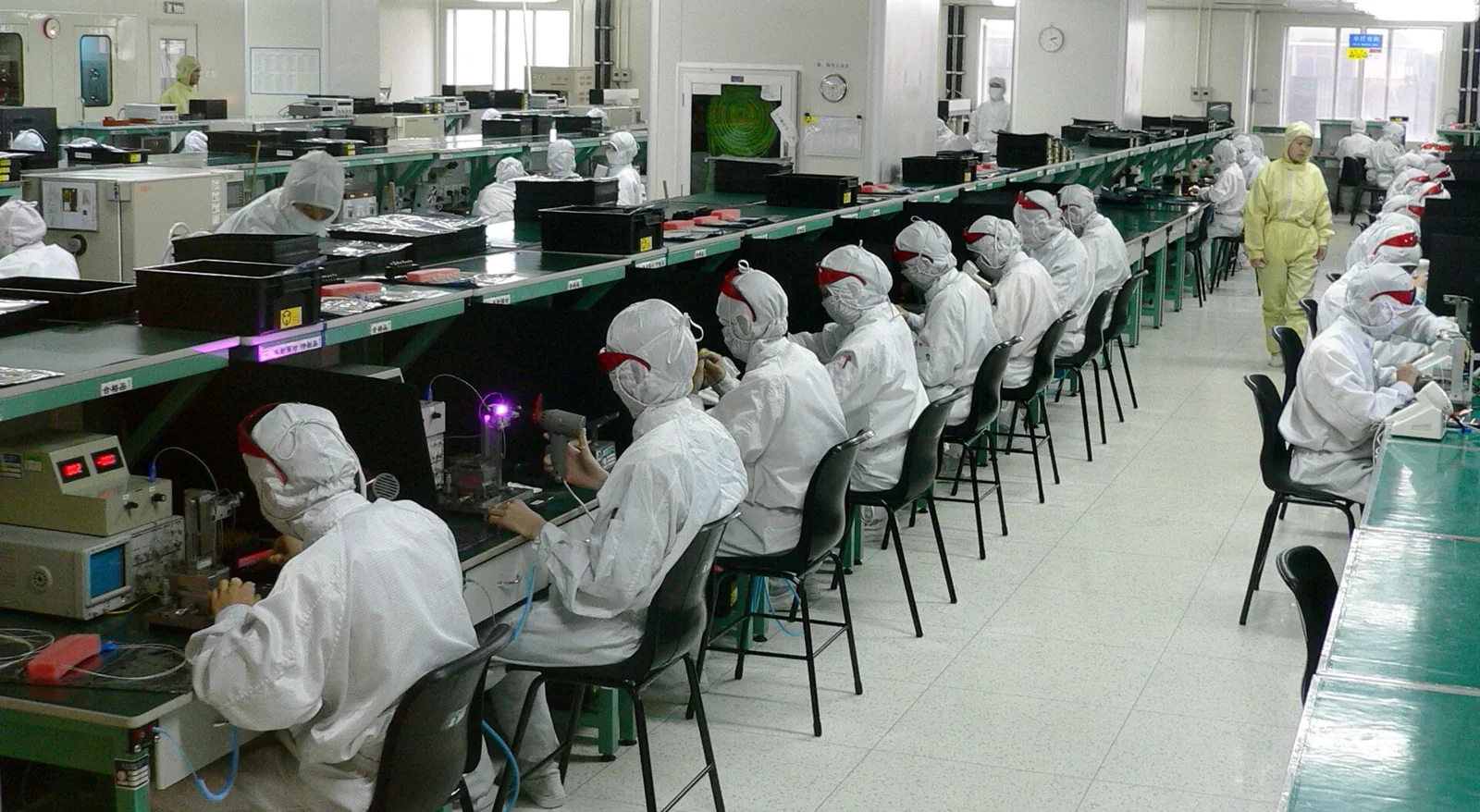
- PCB manufacturing and PCB assembly are two separate processes that share one data package, and most program friction lives at the seam between them, not inside either stage.
- Fabrication produces a bare board; assembly (PCBA) populates it. Each stage consumes specific outputs from the other, so the question is less "who builds it" and more "what travels cleanly between the two."
- One-stop and split sourcing both work, but they fail in different ways. The trade-off is about who owns the data reconciliation and who carries root-cause when a defect crosses the boundary.
- The recurring risk is a mismatch in footprint, stackup, or part revision that is invisible on the bare board and only surfaces when components meet copper at assembly.
- This is a knowledge explainer about the fab-to-assembly handoff. For the actual one-stop service, the routing page is turnkey PCB assembly.
Quick Answer
PCB manufacturing and assemblydescribes two linked stages: fabricating the bare board, then placing and soldering parts onto it. They connect through one shared data set, Gerber or ODB++, BOM, placement, stackup, and test intent. The practical question is not "Can each stage do its job?" It is "Does the data stay consistent as it crosses from fabrication into assembly?" Whether you buy both from one vendor or split them, the seam between fab and assembly is where revision mismatches, footprint errors, and stackup assumptions either get caught early or become rework later.
Table of Contents
- How fabrication and assembly actually connect
- Selection criteria: one-stop vs split fab and assembly
- What data has to travel cleanly between the two stages
- Handoff to a build
- FAQ
- Public references
- Author and review information
How fabrication and assembly actually connect
It helps to stop picturing fabrication and assembly as one continuous line and instead see them as two processes that exchange a defined set of artifacts. Fabrication turns design data into a physical bare board with a fixed stackup, finish, and dimensional profile. Assembly then treats that board as a fixed input and adds components, solder, and test. What one stage outputs becomes what the next stage has to consume without surprises.
| Fabrication stage output | What assembly consumes from it | Why the link matters |
|---|---|---|
| Finished bare board with locked stackup and copper weights | Thermal mass and planarity for reflow profiling | A stackup change that fabrication absorbs quietly can shift how the board heats during soldering |
| Surface finish (ENIG, HASL, OSP, and similar) | Solder paste wetting and joint formation behavior | Finish choice belongs to fabrication but is felt entirely at the assembly bench |
| Solder mask openings and pad geometry | Footprint match against placement and stencil apertures | A pad-to-footprint mismatch is a fabrication-side artifact discovered only when parts are placed |
| Fiducials, tooling holes, panel and break-off design | Machine registration, depaneling, and handling | Panelization decisions made for fabrication directly set assembly machine setup |
| Impedance and controlled-construction notes | Test intent and signal-integrity expectations | Test planning assumes the board was built to the stackup the design called for |
The pattern is that fabrication makes physical commitments, and assembly inherits every one of them. Neither stage can fully validate the other in isolation. That is why a clean fabrication run can still produce an assembly problem: the board is correct against its own data, but that data drifted from what placement and stencil generation assumed. For the fabrication-side view of these stages, the support page is PCB fabrication process, and stackup decisions are detailed at PCB stack-up.
Selection criteria: one-stop vs split fab and assembly
The choice between buying fabrication and assembly together or sourcing them separately is real, and neither answer is universally correct. The decision turns on who carries the data reconciliation between the two stages and who owns root-cause when a defect sits on the boundary. Use the trade-offs below as selection criteria rather than a verdict.
| Decision factor | One-stop (fab + PCBA together) | Split sourcing (separate fab and PCBA) |
|---|---|---|
| Data reconciliation | One party holds both halves of the package, so footprint, stackup, and revision checks happen inside one system | You hold the reconciliation; the assembler verifies a board built by someone else against your data |
| Root-cause ownership | A boundary defect (pad lifted, finish solderability, footprint drift) lands with one accountable team | A board-versus-joint defect can stall between two vendors while each points elsewhere |
| DFM and DFA coupling | Fabrication and assembly review can be run against the same files before build | Each vendor reviews its own scope; coupled issues at the seam can slip through both |
| Supply flexibility | Single relationship, simpler coordination, less freedom to swap one stage | You can pick a specialist fabricator and a specialist assembler, with more sourcing leverage |
| Best fit | Programs where the cost of a cross-vendor mismatch outweighs sourcing flexibility | Programs with mature, frozen data and internal capacity to own the handoff |
A useful way to read this table: one-stop sourcing does not eliminate the fab-to-assembly seam, it just moves the reconciliation inside one vendor's quality system. Split sourcing keeps your sourcing options open but makes you the integrator of the data seam. The DFM intake that supports either model is described at DFM guidelines, and the BOM and component side is at components and BOM.
What data has to travel cleanly between the two stages
This is where most "seamless" promises are actually won or lost. Fabrication data and assembly data, Gerber X2 or ODB++ or IPC-2581, the BOM, placement files, stackup definition, and test intent, are not separate documents that happen to ship together. They describe one board, and they have to stay mutually consistent as they cross from the fabricator to the assembler.
The failure pattern is straightforward to describe and surprisingly common in practice. When that package is handed off in fragments across two vendors, the pieces drift out of sync. A footprint in the placement data no longer matches the pad geometry the fabricator built. A stackup the fabricator adjusted for manufacturability no longer matches the impedance the test plan assumed. A part revision in the BOM no longer matches the footprint on the board. None of this is visible while the board is bare. The mismatch is discovered only at assembly, when components physically meet copper, paste meets pad, and the machine expects registration that the panel does not provide. By then the cost of the fix has changed: it is rework, a fabrication re-spin, or a schedule slip. That is precisely the moment the "seamless" promise fails, at the fab-to-assembly seam, not inside fabrication and not inside assembly.
The data that has to travel cleanly, and stay reconciled, includes:
- fabrication data with explicit stackup intent, not just copper layers
- a BOM whose part revisions match the footprints on the board
- placement data that the assembler can register against the actual panel
- solder mask and pad geometry consistent with the placement footprints
- test intent that reflects the stackup and net list the board was actually built to
Naming the methods at the identity level is enough here. SMT and THT define how parts attach; SPI, AOI, ICT, FCT, and FAI define how the result is checked. The point of listing them is not that any single check certifies the board, but that each one assumes the upstream data was consistent. When the seam holds, those methods do their job. When the seam drifts, they catch the symptom late rather than preventing the cause. The inspection and validation language lives at testing and quality, with first-pass dimensional and build verification at first article inspection and optical defect detection at AOI inspection.
Handoff to a build
When a program moves from understanding the flow to actually building, the useful framing is "what makes the fab-to-assembly handoff reconcilable," not "which vendor is cheapest." A handoff is in good shape when the same data set can be reviewed for fabrication and for assembly without contradiction.
Practical things to confirm before a build:
- the fabrication package and the placement package describe the same footprints, pad geometry, and revision
- the stackup the fabricator will build matches the stackup the test intent assumes
- the BOM part revisions are frozen against the footprints, so SMT and THT placement has no ambiguity
- panelization and fiducials are agreed once, since they serve both depaneling and machine registration
- the validation scope is named at board and process level, not implied as program or end-application qualification
The mechanical and process detail of attachment is covered at SMT and THT assembly. For multi-layer physical bare-board capabilities (4–32 layers), consult our rigid PCB fabrication & manufacturing capabilities, or evaluate early validation runs on prototype PCB manufacturing. If you are consolidating fabrication and assembly under one accountable team specifically to keep this seam inside one quality system, that is the case the turnkey PCB assembly page is built for. When a program is ready to move into intake, the quote path is where files are reviewed against these checks.
FAQ
Are PCB manufacturing and PCB assembly the same thing?
No. PCB manufacturing (fabrication) produces the bare board with its stackup, copper, finish, and profile. PCB assembly, or PCBA, places and solders components onto that finished board and adds inspection and test. They are linked stages that share one data package, not one process.
Why do problems show up at assembly even when the bare board passed?
Because a bare board is verified against its own fabrication data, while assembly verifies the board against the placement, BOM, and test data. If those two halves of the package drifted apart, a footprint, stackup, or revision mismatch stays invisible until parts physically meet copper at the assembly stage.
Is one-stop sourcing always better than splitting fabrication and assembly?
Not always. One-stop sourcing moves the data reconciliation and root-cause ownership inside one vendor, which helps when a cross-vendor mismatch would be costly. Split sourcing keeps sourcing flexibility and lets you pick specialists, but it makes you the integrator of the fab-to-assembly seam.
What data set actually has to stay consistent between the stages?
Fabrication data (Gerber X2, ODB++, or IPC-2581), the BOM, placement files, the stackup definition, and test intent. These describe one board and must stay mutually consistent. A footprint that does not match the built pad, or a part revision that does not match the footprint, is where the handoff breaks.
Do SMT, AOI, ICT, and similar methods guarantee the board is good?
They are identity-level methods for attachment and checking, not guarantees. SMT and THT attach parts; SPI, AOI, ICT, FCT, and FAI check the result against expected data. Each assumes the upstream fabrication and assembly data were consistent, so they verify a build rather than certify reliability on their own.
Who owns a defect that sits on the fab-to-assembly boundary?
In one-stop sourcing, a single team owns boundary defects such as pad geometry, finish solderability, or footprint drift. In split sourcing, ownership can stall between two vendors, so the buyer usually has to define in advance who reconciles the data and carries root-cause at the seam.
Public references
Rigid PCB Fabrication & Manufacturing Support-page context for 4–32 layer rigid PCB fabrication, DFM release gates, and IPC Class 3 tolerances.
Prototype PCB Manufacturing Support-page context for production-intent prototype and NPI readiness review.
PCB fabrication process Support-page context for the fabrication stages that produce the bare board.
PCB stack-up Support-page context for stackup definition and controlled construction planning.
Components and BOM Support-page context for BOM management and component-revision alignment.
DFM guidelines Support-page context for manufacturing review intake and pre-build data alignment.
Testing and quality Support-page context for inspection, validation, and test-planning language at board level.
Turnkey PCB assembly Support-page context for one-stop fabrication and assembly under one quality system.
Author and review information
- Author: APTPCB editorial team
- Technical review: PCBA manufacturing & assembly review team
- Review scope: Fabrication-to-assembly data handoff, sourcing trade-offs, and board-level consistency between fabrication and PCBA stages