Contents
- Highlights
- PCB Prototype Mass Production: Definition and Scope
- PCB Prototype Mass Production Rules and Specifications
- PCB Prototype Mass Production Implementation Steps
- PCB Prototype Mass Production Troubleshooting
- 6 Essential Rules for PCB Prototype Mass Production (Cheat Sheet)
- FAQ
- Request a Quote / DFM Review for PCB Prototype Mass Production
- Conclusion
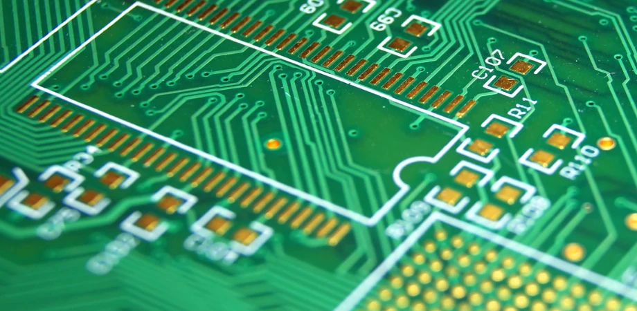
pcb prototype mass production is the critical engineering phase where a functional circuit board design is optimized for high-volume manufacturing. Unlike pure prototyping, which focuses on "making it work" for a few units, mass production focuses on "making it yield" consistently across thousands of units. This transition requires rigorous Design for Manufacturing (DFM) adjustments, supply chain validation, and strict process control to eliminate defects that are invisible in small batches but catastrophic at scale.
Quick Answer
Moving from a prototype to mass production requires shifting your mindset from "feasibility" to "manufacturability." Here are the core tenets for a successful transition:
- Standardize Materials: Switch from generic "FR4" callouts to specific IPC-4101 slash sheets (e.g., /126 for Tg170) to ensure consistent performance across batches.
- Lock the Stackup: Define the exact dielectric thickness and copper weights. Do not leave this to the fabricator's discretion in mass production.
- Panelization is Key: Design your array (panel) for maximum material utilization. Poor panelization can increase costs by 20-30%.
- Verification Rule: Always perform a First Article Inspection (FAI) on the initial pilot run before authorizing the full volume build.
- Pitfall to Avoid: Using "prototype tolerances" (like loose drill wander allowances) in production files. Tighten specs to IPC Class 2 or 3 standards.
- Test Strategy: Implement specific test points for In-Circuit Testing (ICT) or Flying Probe to catch assembly defects early.
- Solder Mask Dams: Ensure a minimum of 4mil (0.1mm) solder mask dams between pads to prevent solder bridging during wave or reflow soldering.
Highlights
- Yield vs. Cost: Understanding how minor design tweaks (like increasing annular rings) can drastically improve yield and lower unit costs.
- Process Consistency: The importance of automated optical inspection (AOI) in maintaining quality across large lots.
- Supply Chain Security: Validating that your Bill of Materials (BOM) components are available in reel quantities, not just cut tape.
- Data Standardization: Converting ambiguous Gerber files into a locked "Production Master" data set.
PCB Prototype Mass Production: Definition and Scope
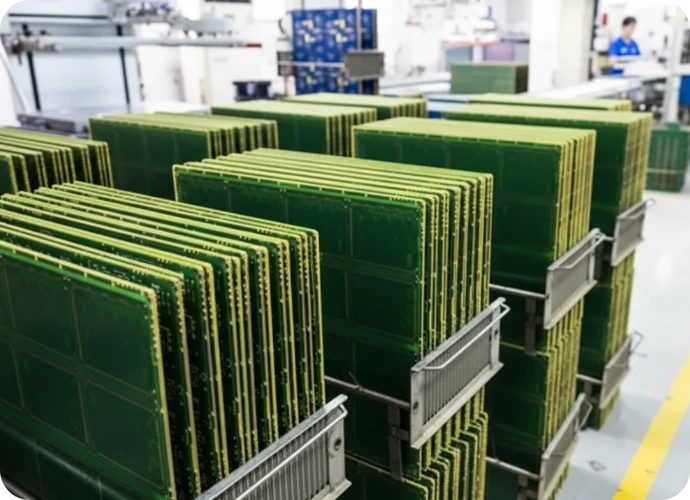
In the context of professional electronics manufacturing, pcb prototype mass production refers to the bridge between New Product Introduction (NPI) and full-scale fabrication. While a prototype proves the electronic logic, the mass production phase proves the process capability.
At APTPCB, we often see designs that work perfectly as a single unit but fail when panelized for assembly. This is usually due to thermal imbalances causing warping during reflow, or component spacing that is too tight for high-speed pick-and-place machines. Mass production involves optimizing the mass production PCB manufacturing workflow to ensure that every board produced matches the "Golden Sample."
This phase also involves "locking" the variables. In prototyping, you might accept a substitute laminate material to get the board faster. In mass production, material substitution is strictly controlled because it affects impedance, thermal expansion, and regulatory compliance (UL/RoHS).
Tech / Decision Lever → Practical Impact
| Decision Lever / Spec | Practical Impact (Yield/Cost/Reliability) |
|---|---|
| Panelization Strategy | Directly impacts material utilization. Efficient nesting can reduce laminate waste and lower unit cost by 15-30%. |
| Surface Finish Selection | ENIG is preferred for fine-pitch BGAs and long shelf life; HASL is cheaper but uneven surfaces reduce assembly yield. |
| Copper Balance | Uneven copper distribution causes bow and twist during reflow, jamming automated assembly lines and causing open joints. |
| Via Technology (HDI vs. Mech) | Moving from mechanical drills to laser microvias increases density but adds cost. Only use HDI if form factor demands it. |
PCB Prototype Mass Production Rules and Specifications
To ensure a smooth transition, your design data must adhere to stricter rules than a quick-turn prototype. Below are the standard specifications we recommend for high-yield production.
| Rule / Parameter | Recommended Value (Standard) | Why it matters | How to verify |
|---|---|---|---|
| Min Trace / Space | 4mil / 4mil (0.1mm) | Going below 4mil requires specialized etching control and lowers yield, increasing cost. | Run DFM check in CAM software (e.g., Genesis, CAM350). |
| Min Mechanical Drill | 0.2mm (8mil) | Drills smaller than 0.2mm break frequently, causing production stoppages and scrap. | Check drill tool list in NC Drill files. |
| Annular Ring | +4mil over hole size | Ensures the drill doesn't break out of the pad (tangency) due to mechanical tolerance. | Verify pad vs. drill diameter in Gerber files. |
| Solder Mask Dam | 4mil (0.1mm) | Prevents solder from flowing between pads (bridging), especially on fine-pitch ICs. | Measure distance between mask openings. |
| Aspect Ratio | 8:1 (Thickness:Hole) | High aspect ratios make plating difficult, leading to barrel cracks or voids. | Calculate board thickness divided by smallest drill size. |
| Bow & Twist | < 0.75% | Warped boards fail in SMT pick-and-place machines and wave soldering conveyors. | PCB Stackup simulation for copper balance. |
PCB Prototype Mass Production Implementation Steps
Transitioning to mass production is a process, not a single event. We follow a structured workflow to mitigate risk.
Implementation Process
Step-by-step execution guide
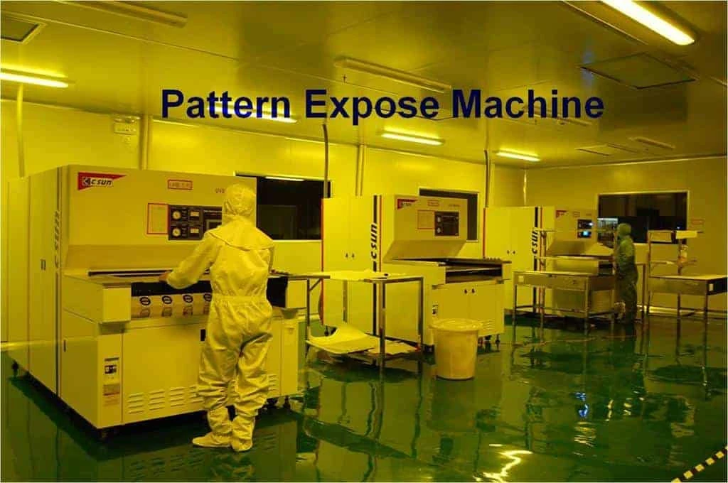
Before cutting metal, our CAM engineers review files for "production killers" like acid traps, slivers, or insufficient thermal relief. This is the "Paper Check" phase.
We clarify ambiguities. E.g., "Is this hole plated or non-plated?" or "Confirm impedance model." Resolving these now prevents scrap later.
A small batch (e.g., 50-100 units) is produced. We perform [First Article Inspection](/en/pcba/first-article-inspection) to verify dimensions, hole quality, and assembly fit.
Once FAI is approved, the process is "locked." No changes to materials or machines are allowed without a formal Engineering Change Order (ECO).
PCB Prototype Mass Production Troubleshooting
Even with careful planning, issues can arise. Here are common failure modes in mass production and how to fix them:
Warping (Bow and Twist):
- Cause: Asymmetrical copper distribution (e.g., a solid plane on layer 2 but sparse traces on layer 3) creates uneven stress during thermal cycles.
- Fix: Use "thieving" (copper pouring) in empty areas of the layout to balance the copper density across the stackup.
Tombstoning (Passive Components):
- Cause: Uneven heating of pads during reflow, often because one pad is connected to a large ground plane without thermal relief.
- Fix: Ensure proper thermal relief connections on all ground pads to balance heat dissipation.
Solder Balling:
- Cause: Solder mask openings are too large, or moisture in the board explodes during reflow.
- Fix: Bake boards before assembly to remove moisture and tighten solder mask expansion rules (typically 2-3mil).
Open Vias:
- Cause: Trapped air or insufficient plating in high-aspect-ratio holes.
- Fix: Reduce aspect ratio or switch to a high-throw plating bath. For reliability, consider filling and capping vias (VIPPO) if they are under BGA pads.
6 Essential Rules for PCB Prototype Mass Production (Cheat Sheet)
| Rule / Guideline | Why It Matters (Physics/Cost) | Target Value / Action |
|---|---|---|
| Copper Balance | Prevents mechanical warping (bow/twist) which jams SMT loaders. | Symmetrical Stackup & Copper Thieving |
| Panel Margins (Rails) | Required for conveyor belts to grip the board during assembly. | 5.0mm - 7.0mm clear edge |
| Fiducial Markers | Allows machines to optically align the board for precise placement. | 3 Global + Local per fine-pitch IC |
| Tooling Holes | Used for test fixtures (ICT) and alignment during fabrication. | 3-4 holes (non-plated, 3.0mm+) in corners |
| Test Point Access | Enables automated electrical testing (ICT/FCT) without manual probing. | Bottom side pads (>0.8mm spacing) |
| Component Spacing | Prevents pick-and-place heads from knocking adjacent parts. | >0.2mm (passives), >0.5mm (ICs) |
FAQ
Q: What is the minimum volume for "mass production"?
A: While definitions vary, we typically consider orders over 50 square meters or 1,000+ units as mass production. However, the process of mass production (locking specs, FAI) should apply to any recurring order, even smaller batches of 100-500 units.
Q: Does mass production reduce the unit price?
A: Yes, significantly. Setup costs (NRE) are amortized over thousands of units. Furthermore, we can optimize panel utilization and purchase materials in bulk, passing savings of 20-40% compared to prototype runs.
Q: Can I change the design after mass production starts?
A: It is highly discouraged. Any change requires a new setup, new stencils, and potentially new test fixtures. This incurs "line down" costs. If a change is necessary, it must go through a strict ECO (Engineering Change Order) process.
Q: How long does the transition from prototype to mass production take?
A: Typically 2-4 weeks. This includes DFM review (2-3 days), Pilot Run fabrication (1-2 weeks), and FAI approval (2-3 days).
Request a Quote / DFM Review for PCB Prototype Mass Production
- Gerber Files: RS-274X or ODB++ format (ensure all layers are aligned).
- BOM (Bill of Materials): Excel format with Manufacturer Part Numbers (MPN).
- Pick & Place File: Centroid data for assembly.
- Fabrication Drawing: PDF specifying material, thickness, color, and special requirements (impedance, blind/buried vias).
- Test Requirements: Specify if ICT, FCT, or burn-in testing is required.
Conclusion
Successfully navigating pcb prototype mass production is about discipline and standardization. By adhering to strict DFM rules, validating your design with a pilot run, and locking down your supply chain, you transform a working prototype into a reliable, profitable product. At APTPCB, our engineering team is ready to guide you through every step of this scaling process, ensuring your transition to volume manufacturing is seamless.
Signed, The Engineering Team at APTPCB