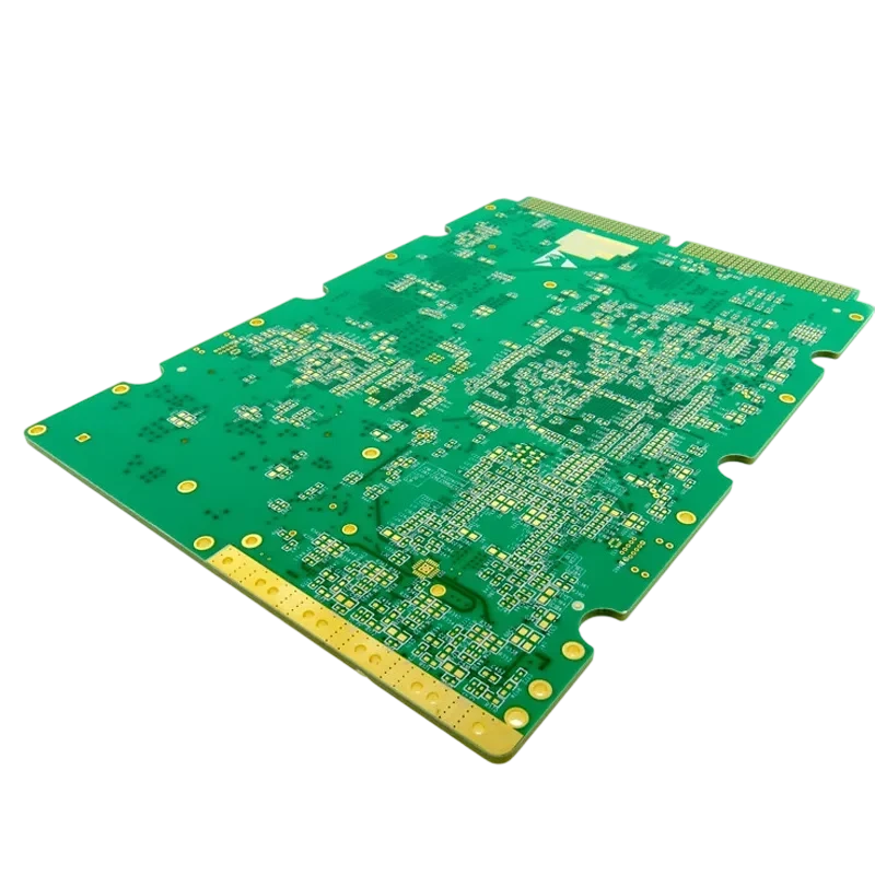
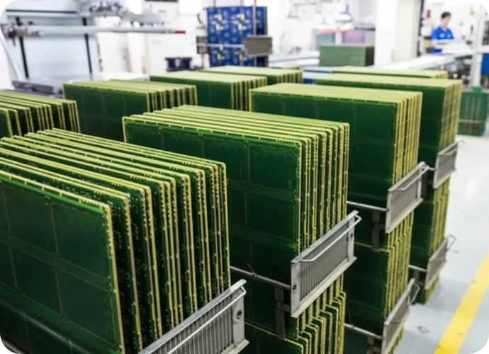
Scaling a design from a functional sample to high-volume manufacturing requires a strategic shift in engineering focus. While pcb prototype mass production might seem like a simple increase in quantity, it fundamentally changes how a board is panelized, sourced, and inspected to guarantee yield and consistency. APTPCB (APTPCB PCB Factory) specializes in bridging this gap, ensuring that designs validated in the lab perform reliably when manufactured by the thousands.
pcb prototype mass production quick answer (30 seconds)
- Objective Shift: Prototypes prioritize speed and proof-of-concept; mass production prioritizes yield, cost-efficiency, and repeatability.
- DFM is Mandatory: A design that works once (prototype) may fail at volume without rigorous Design for Manufacturing (DFM) adjustments.
- Panelization: Production requires optimized panels with tooling rails and fiducials for automated assembly lines, unlike single-unit prototypes.
- Component Sourcing: Move from cut-tape components (digi-key/mouser) to full reels and tray packaging to support high-speed pick-and-place machines.
- Testing Strategy: Implement Automated Optical Inspection (AOI) and In-Circuit Testing (ICT) fixtures rather than manual bench testing.
- Validation: Always perform a First Article Inspection (FAI) and a pilot run (NPI) before committing to full volume to catch systemic errors.
When pcb prototype mass production applies (and when it doesn’t)
Understanding the correct phase for your project prevents wasted capital on tooling or delays due to redesigns.
When it applies:
- Design Freeze: The schematic, BOM, and layout are finalized, and no further functional changes are expected.
- Volume Demand: You anticipate orders exceeding 500–1,000 units where economies of scale significantly reduce unit price.
- Cost Sensitivity: The project requires optimizing the BOM and PCB stack-up to meet a specific target price per unit.
- Standardization: You need consistent performance across thousands of units, requiring strict tolerance controls (impedance, mechanical fit).
- Automated Assembly: The volume justifies the setup cost for stencils, reflow profiling, and test fixtures.
When it doesn’t apply:
- Active Debugging: If you are still cutting traces or swapping resistor values to fix signal integrity issues.
- Low Volume / Custom: Projects requiring only 10–50 units annually are better suited for NPI small batch manufacturing or quick turn services.
- Unverified BOM: If key components are not confirmed for long-term availability (risk of EOL).
- Undefined Testing: If you lack a clear pass/fail criterion for the factory to verify the boards.
- Frequent Iterations: If the product is in a beta phase where user feedback will likely trigger a layout change within a month.
pcb prototype mass production rules and specifications (key parameters and limits)
Transitioning to pcb prototype mass production requires adherence to stricter rules to maximize yield.
| Rule | Recommended value/range | Why it matters | How to verify | If ignored |
|---|---|---|---|---|
| Panelization Efficiency | > 80% material utilization | Reduces waste and cost per unit. | Check panel drawing in Gerber viewer. | Higher unit cost due to wasted FR4 material. |
| Tooling Rails | 5mm - 7mm width | Required for conveyor transport in SMT lines. | Measure edge clearance in CAM files. | Board cannot be assembled automatically; manual handling risks damage. |
| Fiducial Marks | 1mm circle + 2mm clearance | Essential for optical alignment of pick-and-place machines. | Visual check on panel corners and local ICs. | Component placement misalignment; high defect rate. |
| Solder Mask Dam | Min 4 mil (0.1mm) | Prevents solder bridging between pads. | DFM check on fine-pitch ICs. | Short circuits on IC pins during wave/reflow soldering. |
| Surface Finish | ENIG or OSP (for flat pads) | Ensures coplanarity for BGA/fine-pitch parts. | Specify in fabrication notes. | Poor solder joints on BGAs; "black pad" issues if generic HASL is used. |
| Trace Width/Space | Min 4/4 mil (standard) | Standard process is cheaper and higher yield than HDI. | DRC (Design Rule Check) in CAD software. | Increased cost; higher risk of etching defects (opens/shorts). |
| Via Tenting/Plugging | Plugged or Tented | Prevents vacuum loss during ICT testing and solder wicking. | Review solder mask layer. | Solder shorts under BGA; test vacuum failure. |
| Component Spacing | Min 10-20 mil | Allows space for rework and prevents tombstoning. | Assembly DFM review. | Impossible to rework defects; thermal shadowing issues. |
| Copper Balance | Symmetric stack-up | Prevents warping and bowing during reflow heating. | Check layer stack-up symmetry. | Board warps, causing assembly failures or enclosure fit issues. |
| Test Points | > 0.8mm diameter, 2.54mm grid | Enables reliable contact for pogo pins in ICT fixtures. | Overlay test point layer on layout. | Cannot perform automated electrical testing; manual testing is too slow. |
pcb prototype mass production implementation steps (process checkpoints)
Follow this workflow to move from a working prototype to a stable mass production process with APTPCB.
Design Freeze & DFM Review
- Action: Lock the design files and submit for a comprehensive Design for Manufacturing (DFM) review.
- Key Parameter: Identify features that drive up cost (e.g., blind vias, tight tolerances) and relax them if possible.
- Acceptance Check: DFM report shows zero critical errors; engineering questions (EQ) are resolved.
BOM Scrub & Availability Check
- Action: Verify all components are available in production volumes (reels) and identify second sources for passives.
- Key Parameter: Component Lead Time and Lifecycle status (Active vs. NRND).
- Acceptance Check: BOM is 100% sourceable with no obsolete parts.
Panelization Design
- Action: Create a panel array (e.g., 2x5) with break-away tabs (mouse bites) or V-scores.
- Key Parameter: Panel size must fit the SMT machine limits (typically max 500mm x 400mm).
- Acceptance Check: Panel drawing approved by assembly engineers.
First Article Inspection (FAI)
- Action: Produce a small number of units (5–10) using the mass production tooling and process.
- Key Parameter: First Article Inspection report comparing the physical board against the BOM and Gerber.
- Acceptance Check: FAI report signed off; functional test passed.
Pilot Run (NPI)
- Action: Run a small batch (50–100 units) to validate the process capability (Cpk) and test fixtures.
- Key Parameter: Yield rate (target > 98% first pass yield).
- Acceptance Check: No systemic defects found; test fixtures calibrated.
Mass Production Release
- Action: Authorize full volume production based on the locked process from the pilot run.
- Key Parameter: Weekly/Monthly output rate.
- Acceptance Check: Consistent delivery schedule and quality metrics met.
pcb prototype mass production troubleshooting (failure modes and fixes)
When scaling to pcb prototype mass production, new failure modes appear that were not visible in hand-soldered prototypes.
Symptom: Tombstoning (Passive components standing up)
- Causes: Uneven heating during reflow; unbalanced copper pads (one side connected to large ground plane).
- Checks: Inspect thermal relief connections on ground pads.
- Fix: Add thermal spokes to ground pads; adjust reflow profile.
- Prevention: Adhere to strict footprint design guidelines for mass production.
Symptom: PCB Warpage / Bow and Twist
- Causes: Asymmetric copper distribution in layer stack-up; thin core material (< 0.8mm).
- Checks: Measure bow percentage against IPC standards (< 0.75%).
- Fix: Use a heavier pallet during reflow; bake boards before assembly to remove moisture.
- Prevention: Ensure copper balance in design; choose high Tg materials for lead-free processes.
Symptom: BGA Head-in-Pillow (HiP)
- Causes: Warpage causing BGA ball to separate from paste; poor wetting.
- Checks: X-ray inspection; cross-section analysis.
- Fix: Adjust reflow soak time; switch to high-activity solder paste.
- Prevention: Use DFM guidelines to ensure proper BGA pad size and mask opening.
Symptom: Solder Bridging on Fine Pitch ICs
- Causes: Stencil aperture too large; solder mask web too thin.
- Checks: Inspect stencil thickness and aperture reduction.
- Fix: Clean stencil more frequently; reduce aperture size by 10%.
- Prevention: Ensure solder mask dams exist between pins in the PCB layout.
Symptom: Inconsistent Impedance
- Causes: Variation in dielectric thickness or trace width etching during fabrication.
- Checks: TDR (Time Domain Reflectometry) measurement on coupons.
- Fix: Adjust stack-up or trace width in CAM engineering.
- Prevention: Specify impedance control requirements clearly in fabrication notes.
Symptom: Cracked MLCC Capacitors
- Causes: Mechanical stress during depanelization (breaking boards apart).
- Checks: Inspect capacitor orientation relative to V-score/break lines.
- Fix: Change depanelization method to router/milling.
- Prevention: Place capacitors parallel to break lines or move them away from edges.
How to choose pcb prototype mass production (design decisions and trade-offs)
Strategic choices made during the design phase dictate the success of pcb prototype mass production.
- Material Selection: For prototypes, standard FR4 is fine. For production, consider if you need High Tg material (Tg170) to withstand multiple thermal cycles (reflow + wave + rework) without delamination.
- Surface Finish: HASL is cheap but uneven. ENIG (Electroless Nickel Immersion Gold) costs more but provides a flat surface essential for BGAs and ensures longer shelf life for bare boards.
- Test Strategy: Deciding between ICT (In-Circuit Test) and FCT (Functional Test). ICT requires specific pad designs (test points) added during layout but offers faster throughput for high volumes. FCT is slower but verifies actual operation.
- Panelization Strategy: V-score is faster and cheaper but requires straight lines. Tab-routing allows complex shapes but leaves small nubs that may need sanding.
- Component Selection: Avoid "single source" components. Always design with alternatives in mind to prevent line-down situations if a specific part goes out of stock.
pcb prototype mass production FAQ (cost, lead time, may fail at volume without rigorous Design for Manufacturing (DFM) files, stackup, impedance, Implement Automated Optical Inspection (AOI) inspection)
1. Can I use the exact same Gerber files for prototype and mass production? Generally, yes, but you should update them based on DFM feedback. Prototypes often lack panelization, fiducials, or optimized thermal reliefs that are critical for automated assembly.
2. What is the typical lead time difference? Quick turn PCB prototypes can be done in 24–48 hours. Mass production typically requires 10–15 days for PCB fabrication plus additional time for component procurement and assembly setup.
3. Do I need to pay for tooling again? If you change the design (even slightly), yes. If the design is identical, production tooling (E-test fixtures, stencils) is usually a one-time cost, though mass production tooling is more durable and expensive than prototype tooling.
4. How do you handle EOL (End of Life) components during production? We monitor BOM health. If a part goes EOL, we propose a drop-in replacement or a "last time buy" strategy. This highlights the importance of a BOM scrub before starting mass production.
5. What is the minimum volume for "Mass Production"? There is no strict cutoff, but "Mass Production" processes (like full automation) usually become cost-effective above 500–1,000 units. Below that, NPI small batch manufacturing is often more appropriate.
6. Why is the unit price lower in mass production? Setup costs (CAM, stencils, machine programming) are amortized over thousands of units. Additionally, material utilization is optimized, and assembly lines run continuously, reducing labor cost per board.
7. Should I use hard gold or ENIG? Use Hard Gold for edge connectors that will be plugged/unplugged frequently. Use ENIG for the rest of the board to ensure solderability and flatness for SMT components.
8. What is a "Golden Sample"? A Golden Sample is a perfectly manufactured and tested unit from the pilot run kept as a reference standard for quality control in future production batches.
9. How do I specify impedance control? Include an impedance table in your fabrication drawing specifying the target impedance (e.g., 50Ω), the trace width, layer, and reference plane. We will adjust the stack-up to match.
10. Can you handle partial shipments? Yes. For large mass production orders, we can manufacture the full batch to secure pricing and schedule partial deliveries (kanban) to manage your inventory levels.
pcb prototype mass production glossary (key terms)
| Term | Definition |
|---|---|
| NPI | New Product Introduction; the process of taking a design from prototype to production. |
| DFM | Design for Manufacturing; optimizing a design to be easily and cheaply manufactured. |
| DFA | Design for Assembly; optimizing a design to be easily assembled (components placed/soldered). |
| FAI | First Article Inspection; verification of the first unit produced to ensure process correctness. |
| Panelization | Grouping multiple PCBs onto a larger panel to increase manufacturing throughput. |
| Fiducial | Optical markers on the PCB used by assembly machines for alignment. |
| Mouse Bites | Perforated break-away tabs used to separate individual boards from a panel. |
| Pick and Place | The automated process of picking components from reels and placing them on the PCB. |
| Reflow Profile | The temperature-vs-time curve used in the reflow oven to melt solder paste. |
| Yield Rate | The percentage of manufactured boards that pass testing without defects. |
| MOQ | Minimum Order Quantity; the smallest number of units a factory is willing to produce. |
| Gerber File | The standard file format used to describe PCB layers (copper, mask, silk) to the factory. |
Request a quote for pcb prototype mass production (may fail at volume without rigorous Design for Manufacturing (DFM) review + pricing)
Ready to scale? APTPCB provides seamless transition support from prototype to volume manufacturing.
- Get a Quote: Contact us today for a full DFM review and mass production pricing strategy.
- What to send: Please provide Gerber files (RS-274X), BOM (Excel format with manufacturer part numbers), Pick & Place file (XY coordinates), and any special assembly drawings or test procedures.
Conclusion (next steps)
Successfully navigating pcb prototype mass production is about risk management and process control. By validating your design with rigorous DFM checks, establishing clear quality criteria, and partnering with an experienced manufacturer like APTPCB, you ensure your product scales efficiently. Whether you need 50 complex boards or 50,000 standard units, following these specifications will secure your timeline and budget.