Understanding PCB Stackup Design and Why It Matters
Before you talk about DDR routing, SERDES length matching, or via fan-outs, one quiet decision is already shaping your success: your PCB stackup. Layer order, plane placement, and dielectric choices decide how easy it is to control impedance, keep return paths clean, and pass EMI the first time.
A stackup is not just “how many layers” you pay for. It’s the electrical architecture of the board: which signals sit next to solid ground, where power rails are distributed, how tightly loops can be closed, and how your design will behave once it leaves the simulator and hits the real factory line.
At APTPCB, we treat stackup design as a shared engineering task, not a last-minute checkbox. Our team reviews your requirements and proposes PCB stackup examples that line up with real materials, real process capabilities, and your SI/PI targets – from simple 4-layer concepts to 64-layer advanced multi-layer laminated structures.
Key Considerations in PCB Stackup Design
- Signal Integrity (SI):
The placement of signal layers relative to reference planes controls impedance, reflections, and crosstalk. A well-designed stackup gives high-speed nets a stable, predictable environment. - Power Integrity (PI):
Power and ground plane pairs form the core of the PDN. Plane spacing, thickness, and segmentation influence decoupling performance, rail noise, and transient behavior. - Return Path Control:
Every signal needs a clean return. Stackups that keep signals close to intact ground planes reduce loop area, lower inductance, and minimize EMI problems. - Material Selection:
FR-4, high-Tg, and low-loss materials each have different Dk/Df and processing characteristics. The stackup is where electrical requirements meet real-world PCB fabrication processes. - Manufacturability and Cost:
The best stackup is one you can build repeatedly. Layer count, copper weight, and dielectric thickness must sit inside reliable process windows and a realistic budget. - Future Scalability:
A stackup that works “just barely” today may fail when speeds or functionality increase. Good stackup design anticipates future interfaces and reuse across product variants.
Reliable Performance Starts with the Stackup
By addressing these points up front, APTPCB helps you avoid the classic situation where a layout looks fine but fails SI, PI, or EMI late in the project. Instead of guessing, you start from validated PCB stackup examples that already align with material availability, drill rules, and quality targets.
This approach shortens design cycles, reduces the number of board spins, and gives your team a stable electrical foundation to build on – whether you’re working on a compact IoT controller or a high-layer server backplane.
Practical PCB Stackup Examples from 4 to 12 Layers
Most engineering teams don’t design a stackup from zero each time. Instead, they begin from proven PCB stackup examples and adapt them to their own signals, power rails, and mechanical constraints. Having a clear library of 4-, 6-, 8-, 10-, and 12-layer PCB stackup examples saves time and reduces risk.
At APTPCB, we use a set of battle-tested reference stackups as starting points for customer projects. These are not rigid templates; they are practical patterns that have already survived fabrication, assembly, and field use.
Key PCB Stackup Examples (4–12 Layers)
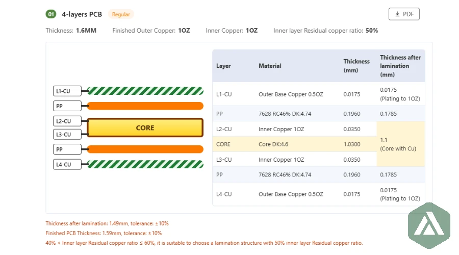
4-Layer PCB Stackup Example – Cost-Effective Baseline
Typical 4-layer PCB stackup example:
Top Signal / Inner Ground / Inner Power / Bottom Signal.
Good for cost-sensitive designs that still need a solid ground plane and basic controlled impedance.
Common in consumer products and simple embedded systems.6-Layer PCB Stackup Example – Better Isolation and PDN
Typical 6-layer PCB stackup example:
Top Signal / Inner Ground / Inner Signal / Inner Power / Inner Ground / Bottom Signal.
Adds routing capacity and greatly improves isolation and PDN performance.
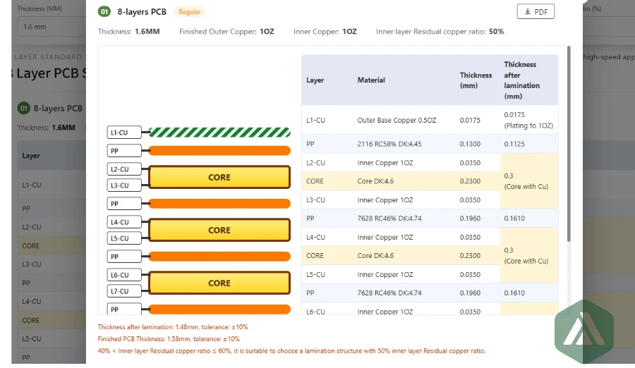
Suitable for more complex digital boards and mid-speed interfaces.8-Layer PCB Stackup Examples – High-Speed Oriented
Popular 8-layer PCB stackup examples use multiple ground planes, for example:
Top Signal / GND / Inner Signal / PWR / GND / Inner Signal / GND / Bottom Signal.
Excellent for high-speed buses, SERDES, and dense differential pairs, where tight impedance control and strong shielding are required.10-Layer PCB Stackup Example – Dense Routing and Many Interfaces
A 10-layer PCB stackup example typically adds extra inner signal layers while preserving several power and ground planes.
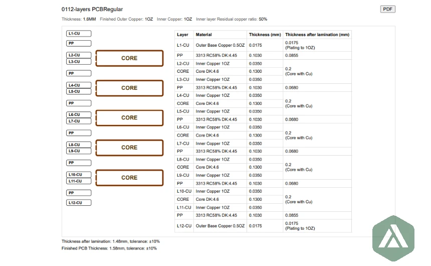
This is a solid choice for high-performance computing boards, networking equipment, and large FPGA designs with many I/O standards.12-Layer PCB Stackup Examples – Multiple Power Domains and Strict EMI
For boards with many power rails, complex buses, and tough EMI limits, 12-layer PCB stackup examples provide maximum flexibility.
Extra planes make it easier to isolate noisy subsystems, while extra signal layers keep routing manageable even at high density.Advanced PCB Stackup Examples for High-Speed and RF
When you move into very high-speed or RF designs, classic FR-4 stackups may not be enough. We offer high-speed advanced PCB manufacturing stackup examples that introduce low-loss materials, tuned dielectrics, and carefully paired reference planes.
Using Examples as Smart Starting Points
The goal of sharing PCB stackup examples is not to encourage copy-paste design, but to give you realistic starting points that are already compatible with manufacturing. You can then adjust layer assignments, copper weights, or materials without breaking the fundamentals.
When you send your schematic and constraints to APTPCB, our engineers will often begin from one of these reference stackups, then refine it based on your interfaces, power rails, and mechanical outline. This keeps the conversation concrete – you’re always looking at a real, buildable stackup, not just a theoretical drawing.
Custom PCB Stackup Examples for Controlled Impedance and High-Speed Design
Once you start dealing with multi-gigabit links, RF sections, or very tight timing budgets, generic stackups are no longer enough. At that stage, you need custom PCB stackup examples that are calculated specifically for your impedance targets, materials, and routing constraints.
Standard FR-4 may still be part of the picture, but now you are also thinking about loss tangent, glass weave, copper roughness, and detailed via structures. Every layer spacing and dielectric choice shows up in eye diagrams, insertion loss plots, and compliance tests.
Key Elements of Custom High-Speed PCB Stackup Examples
Controlled Impedance Targets:
Custom PCB stackup examples start from real impedance goals, such as 50 Ω single-ended or 85/100 Ω differential. Dielectric thickness, trace width, and materials are tuned to hit those numbers with margin.Material Systems (FR-4, High-Tg, Low-Loss):
Depending on your frequency and channel length, we combine standard FR-4 with higher-grade materials. Low-loss laminates, high-Tg cores, and spread-glass options are selected based on your signal-integrity budget.Layer Pairing for Signal and Reference:
High-speed PCB stackup examples always keep critical traces closely coupled to solid reference planes. We minimize reference changes and design return paths consciously, especially under BGA fan-outs and dense breakout regions.Via Strategy and HDI Options:
Through-hole, blind, buried, and microvia combinations all affect impedance and manufacturability. Custom stackup examples integrate the via concept – including possible backdrilling – so routing and signal integrity align with drill capabilities.Power Distribution Network (PDN) Optimization:
Power and ground plane spacing, decoupling locations, and plane shapes are part of the stackup definition. For noisy or high-current designs, we adjust the PDN with both simulation and real PCB stackup examples from similar products.Alignment with Fabrication Limits:
All of the above is constrained by what can be fabricated reliably. Minimum dielectric thickness, copper distribution, and lamination cycles must be compatible with our real production lines and yield targets.
From Concept to Fabricated High-Speed Boards
When you share your interface list, data rates, and mechanical outline with APTPCB, we can propose one or more custom PCB stackup examples tailored to your product. We use field-solver data, material datasheets, and internal process windows to ensure the numbers are realistic.
Because these custom stackups are created together with our PCB fabrication team, you avoid the classic gap between “simulated” and “buildable”. The result is a board that behaves as expected in the lab and can be produced at scale with stable PCB quality.
Choosing a PCB Manufacturer for Complex Stackups up to 64 Layers
The more layers and interfaces your design has, the more your stackup success depends on the real capabilities of the factory that will build it. A basic 4-layer PCB stackup design can be produced by many suppliers—but a 32- or 64-layer impedance-controlled structure with HDI and mixed dielectric materials requires a manufacturer with deep engineering experience and mature process control.
You need a partner who treats stackup design as an engineering discipline, not a cost checkbox. This means receiving actionable feedback on feasibility, risk points, material choices, and long-term manufacturability before you commit to expensive prototypes.
Key Criteria When Selecting a Stackup-Capable PCB Partner
- Layer-Count and HDI Experience: Ensure the manufacturer has proven capability with high-layer and HDI boards—not just standard FR-4. Ask for their experience with 10-, 12-, 16-layer and higher stackup design, including HDI build-up structures.
- Material and Stackup Engineering Support: Choose a team that can propose and refine PCB stackup designs—covering FR-4, high-Tg, hybrid builds, and low-loss laminates—rather than simply accepting or rejecting your submitted stackup drawing.
- DFM and NPI Services: Early DFM (Design for Manufacturability) review helps identify risks related to dielectric thickness, drill constraints, copper balance, and lamination cycles. APTPCB’s NPI and small-batch PCB manufacturing platform is designed to validate and fine-tune stackup designs before scaling to mass production.
- Test and Quality Infrastructure: Impedance coupons, cross-sectioning, reliability testing, and material traceability are essential when validating complex stackup designs, especially for 32–64 layer boards.
- Communication and Iteration Speed: Stackup definition is iterative. Choose a partner who responds quickly with updated PCB stackup design options, material alternates, and quantified trade-offs for cost, performance, and manufacturability.
- Scalability from Prototype to Volume: A successful PCB stackup design must remain stable from prototype to large-scale production. Ensure the factory’s processes, materials, and lamination equipment can maintain consistency across the entire product lifecycle.
Turning PCB Stackup Design into Production-Ready Hardware
APTPCB supports everything from simple 4-layer stackup designs to advanced builds with up to 64 layers, controlled impedance, HDI microvia structures, and hybrid materials. We help customers move from initial PCB stackup design through NPI verification and into stable mass production—without unexpected redesigns or material changes.
By treating stackup engineering as a shared responsibility, we help you avoid late-stage SI/PI failures, EMI issues, manufacturability problems, and yield loss. The result is a robust board structure that:
- aligns with electrical and mechanical requirements
- fits within proven fabrication windows
- can be reproduced consistently throughout the product lifecycle
If you are planning a new design or want to review an existing one, send us your layer count, interfaces, speed grades, material constraints, and target performance. Our engineering team will propose optimized PCB stackup design options you can use immediately in your project.