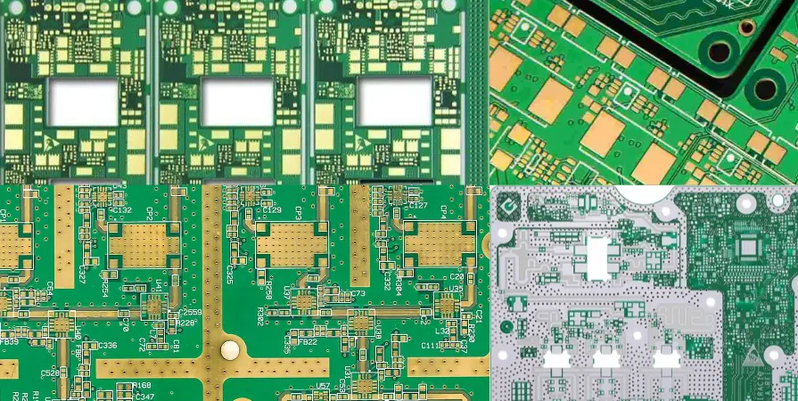
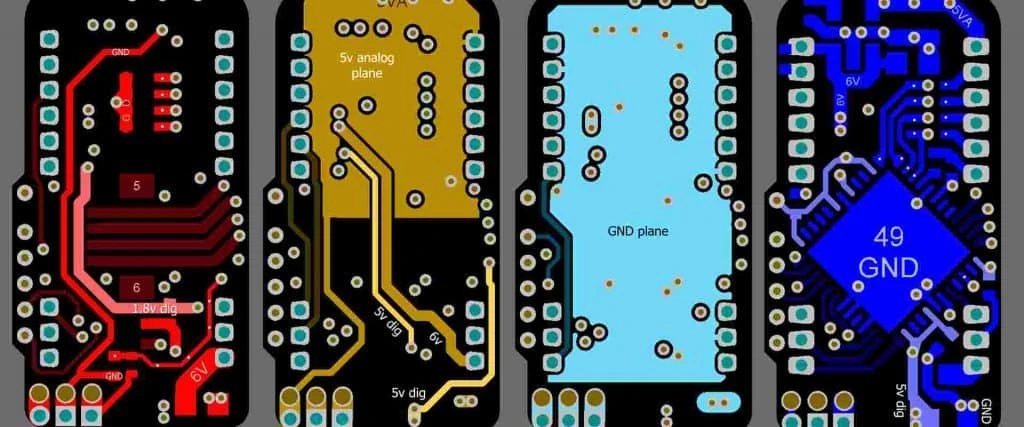
Effective pcb stackup design is the foundation of every reliable electronic device, determining signal integrity, power delivery, and manufacturability before a single trace is routed. It involves the precise arrangement of copper layers and insulating materials (dielectrics) to meet specific electrical and mechanical requirements. At APTPCB (APTPCB PCB Factory), we see stackup planning as the most critical phase in the engineering workflow. This guide covers everything from basic definitions to advanced validation techniques.
Key Takeaways
- Definition: It is the vertical arrangement of copper layers and dielectric materials (Core and Prepreg) in a printed circuit board.
- Signal Integrity: Proper stackups minimize crosstalk and electromagnetic interference (EMI) while maintaining controlled impedance.
- Symmetry is Vital: Balanced copper distribution prevents board warpage during the reflow soldering process.
- Material Selection: The choice between standard FR4 and high-frequency materials (like Rogers) dictates performance and cost.
- Validation: Always simulate the stackup and confirm material availability with your manufacturer before routing.
- Cost Driver: Layer count and blind/buried via technologies significantly impact the final unit price.
What pcb stackup design really means (scope & boundaries)

Building on the key takeaways, understanding the scope of a stackup helps engineers avoid over-engineering or under-performing designs. pcb stackup design is not just about counting layers; it is the architectural blueprint of the circuit board.
It encompasses the selection of the dielectric constant (Dk), the determination of layer spacing, and the assignment of signal versus plane layers. A robust stackup manages the return paths for high-speed signals and provides a stable power delivery network. If the stackup is flawed, even the most perfect routing cannot save the board from signal failures or excessive emissions.
pcb stackup design metrics that matter (how to evaluate quality)
Once you understand the scope, you must evaluate the design against specific measurable metrics.
| Metric | Why it matters | Typical range or influencing factors | How to measure |
|---|---|---|---|
| Impedance (Z0) | Matches source and load to prevent signal reflection. | 50Ω (Single), 90Ω/100Ω (Diff Pair). | TDR (Time Domain Reflectometry). |
| Dielectric Constant (Dk) | Affects signal propagation speed and trace width requirements. | 3.0 to 4.5 (FR4 varies by resin content). | Material datasheet / Impedance solver. |
| Glass Transition (Tg) | Determines the temperature at which the PCB becomes mechanically unstable. | 130°C (Standard) to 180°C+ (High Tg). | TMA (Thermal Mechanical Analysis). |
| Layer Symmetry | Prevents bowing and twisting during assembly. | Balanced copper weight and dielectric thickness from center. | Flatness test / Visual inspection. |
| Copper Weight | Dictates current carrying capacity and trace etching resolution. | 0.5 oz to 2.0 oz (standard); up to 10 oz (heavy). | Cross-section analysis. |
| Loss Tangent (Df) | Critical for signal attenuation in high-frequency designs. | 0.02 (Standard FR4) to 0.001 (PTFE). | VNA (Vector Network Analyzer). |
How to choose pcb stackup design: selection guidance by scenario (trade-offs)
With the metrics defined, the next step is selecting the right configuration based on your specific application requirements.
1. Standard 4-Layer (Cost-Sensitive)
- Scenario: Consumer electronics, simple microcontrollers, low-speed interfaces.
- Trade-off: Low cost vs. limited routing space and EMI shielding.
- Configuration: Signal / Ground / Power / Signal. This is the most common entry-level stackup.
2. High-Speed Digital (Signal Integrity Focus)
- Scenario: DDR memory, PCIe interfaces, Gigabit Ethernet.
- Trade-off: Higher layer count (6-12 layers) vs. excellent signal quality.
- Configuration: Alternating signal and ground layers. Stripline routing is preferred for EMI containment.
3. High-Density Interconnect (Size Constraint)
- Scenario: Smartphones, wearables, compact IoT devices.
- Trade-off: High manufacturing cost vs. extreme miniaturization.
- Configuration: Uses microvias, blind/buried vias, and fine pitch BGA support. See our HDI PCB capabilities for details on build-up layers.
4. RF and Microwave (Frequency Focus)
- Scenario: Radar, 5G antennas, satellite communications.
- Trade-off: Expensive materials vs. low signal loss.
- Configuration: Hybrid stackups using Rogers materials on the outer layers and standard FR4 inside for mechanical stability.
5. High Power Distribution (Current Focus)
- Scenario: Power supplies, automotive inverters, battery management systems.
- Trade-off: Thicker copper (harder to etch fine lines) vs. high current capacity.
- Configuration: Heavy copper inner layers (2oz+) dedicated to power planes.
6. Rigid-Flex (Mechanical Focus)
- Scenario: Foldable devices, aerospace sensors, complex enclosures.
- Trade-off: Complex fabrication process vs. elimination of connectors.
- Configuration: Flexible polyimide layers integrated into the rigid FR4 stackup.
pcb stackup design implementation checkpoints (design to manufacturing)

After selecting the scenario, you must execute the design using a rigorous checklist to ensure manufacturability.
- Symmetry Check: Ensure the stackup is symmetrical around the center core.
- Risk: Board warping during reflow.
- Acceptance: Balanced dielectric thickness and copper weights.
- Core vs. Prepreg Arrangement: Verify the manufacturer's preferred construction (foil-build vs. core-build).
- Risk: Incorrect final thickness or impedance.
- Acceptance: Confirm with APTPCB engineering support.
- Impedance Trace Widths: Calculate trace widths based on the actual material Dk, not generic values.
- Risk: Signal reflections and data loss.
- Acceptance: Use a field solver or our impedance calculator.
- Reference Planes: Ensure every high-speed signal layer has an adjacent solid reference plane (GND).
- Risk: High EMI and crosstalk.
- Acceptance: Visual check of layer adjacency.
- Material Availability: Confirm the specific laminates are in stock.
- Risk: Long lead times or forced redesigns.
- Acceptance: Supplier confirmation email.
- Copper Balance: Fill empty areas on signal layers with copper pour (thieving).
- Risk: Uneven plating thickness.
- Acceptance: Copper density map > 70% uniformity.
- Via Aspect Ratio: Keep via depth-to-diameter ratio under 10:1 for standard plating.
- Risk: Reliable plating failure (open circuits).
- Acceptance: Drill chart verification.
- Resin Content: Ensure prepreg layers have enough resin to fill inner layer copper voids.
- Risk: Delamination or voids (measling).
- Acceptance: High-resin prepreg selection for heavy copper layers.
- Total Thickness Tolerance: Define the acceptable tolerance (usually ±10%).
- Risk: Mechanical fit issues in the enclosure.
- Acceptance: Stackup calculation summary.
- Blind/Buried Via Definition: Clearly define start and stop layers in the Gerber files.
- Risk: Manufacturing errors or scrapped boards.
- Acceptance: Drill table explicitly states layer pairs.
pcb stackup design common mistakes (and the correct approach)
Even with a checklist, engineers often fall into specific traps during the implementation phase.
- Mistake 1: Relying on Datasheet Dk Values.
- Correction: Datasheet Dk is often tested at 1 MHz. For high-speed designs, use the Dk value at your operating frequency (e.g., 1 GHz or 10 GHz).
- Mistake 2: Asymmetric Stackups.
- Correction: Never mix different copper weights on symmetrical layers (e.g., Layer 2 is 1oz, Layer 3 is 0.5oz). Keep them identical to prevent twisting.
- Mistake 3: Ignoring Return Paths.
- Correction: Routing a signal over a split plane creates a large loop area. Always route over a solid ground plane.
- Mistake 4: Over-specifying Materials.
- Correction: Do not specify "Rogers 4350B" if standard FR4 works for your frequency. It triples the cost unnecessarily.
- Mistake 5: Neglecting Prepreg Thickness Changes.
- Correction: Prepreg thins out as resin flows between traces during lamination. Account for "pressed thickness" rather than "nominal thickness."
- Mistake 6: Mixing Units.
- Correction: Stick to either metric (mm/um) or imperial (mils/oz) throughout the stackup document to avoid conversion errors.
pcb stackup design FAQ (cost, lead time, materials, testing, acceptance criteria)
Addressing common mistakes often leads to specific questions regarding logistics and validation.
1. How does pcb stackup design impact the final board cost? Cost increases with layer count, the use of exotic materials (like PTFE), and the inclusion of blind/buried vias. A standard 4-layer FR4 board is significantly cheaper than an 8-layer HDI board.
2. What is the lead time impact of a custom stackup? If you use standard materials (FR4, standard copper weights), there is no delay. However, specifying non-stocked dielectrics or odd copper weights can add 1-3 weeks to the lead time for material procurement.
3. gcpw vs microstrip vs stripline: when to use which?
- Microstrip: Outer layer trace. Best for ease of routing and component placement.
- Stripline: Inner layer trace sandwiched between grounds. Best for EMI suppression and high-speed signals.
- GCPW (Grounded Coplanar Waveguide): Outer layer with adjacent grounds. Best for RF applications requiring high isolation.
4. How do I validate the stackup before ordering? Perform a controlled impedance stackup checklist review. Send your proposed stackup to the fabrication house during the quoting phase for a DFM (Design for Manufacturing) check.
5. Can I mix materials in a hybrid stackup? Yes. This is common in RF designs where the top layer is a high-frequency material and the inner layers are FR4 to save cost. However, the materials must have compatible CTE (Coefficient of Thermal Expansion) to prevent delamination.
6. What are the acceptance criteria for stackup thickness? IPC-6012 specifies a standard thickness tolerance of ±10%. For controlled impedance boards, the dielectric thickness is critical and may require tighter process controls.
7. Why is "pressed thickness" different from "nominal thickness"? Nominal thickness is the raw material size. Pressed thickness is the final size after the lamination cycle, where resin flows into the gaps between copper tracks. Impedance calculations must use pressed thickness.
8. Does copper roughness affect pcb stackup design? Yes, for very high-speed signals (10Gbps+). Rough copper increases skin effect losses. You may need to specify "VLP" (Very Low Profile) or "HVLP" copper foil in the stackup notes.
Resources for pcb stackup design (related pages and tools)
- Impedance Calculator: Use our online tool to estimate trace widths.
- Material Datasheets: Access specifications for Isola, Rogers, and Panasonic materials.
- DFM Guidelines: Download our comprehensive design guide.
- Quote System: Upload your Gerber files and stackup for an instant review.
pcb stackup design glossary (key terms)
To effectively communicate with manufacturers, you must master the terminology used in stackup documents.
| Term | Definition |
|---|---|
| Core | A rigid base material with copper cured on both sides. The "skeleton" of the PCB. |
| Prepreg | Fiberglass fabric impregnated with semi-cured resin. It bonds cores together. |
| Foil | Thin sheets of copper added to the outer layers or built up on prepreg. |
| Stackup | The map of layers, materials, and thicknesses in a PCB. |
| Dielectric Constant (Dk) | A measure of a material's ability to store electrical energy in an electric field. |
| Dissipation Factor (Df) | A measure of how much signal energy is lost as heat in the material. |
| Microstrip | A transmission line on an outer layer referenced to a single plane below it. |
| Stripline | A transmission line on an inner layer sandwiched between two reference planes. |
| Blind Via | A via connecting an outer layer to an inner layer, not going through the whole board. |
| Buried Via | A via connecting inner layers only, invisible from the outside. |
| CTE | Coefficient of Thermal Expansion. How much the material expands under heat. |
| Balanced Stackup | A stackup where layers are mirrored from the center to prevent warping. |
Conclusion (next steps)
Mastering pcb stackup design is the difference between a prototype that works on the first spin and one that requires costly revisions. By focusing on symmetry, understanding material properties, and validating impedance early, you ensure a smooth transition from engineering to mass production.
When you are ready to move forward, APTPCB is here to assist. To get the most accurate pricing and engineering support, please provide the following when you Get a quote:
- Gerber files (RS-274X).
- A stackup drawing or text description (layer count, finished thickness).
- Impedance requirements (if any).
- Material specifications (Tg, specific brands if required).
A well-planned stackup is the first step toward product success.