
Definition, scope, and who this guide is for
Defining a robust quality control plan is the first step to preventing field failures, and this guide breaks down the four pillars of modern inspection. A comprehensive pcba testing strategy: aoi xray ict fct combines visual, structural, electrical, and functional verification to ensure zero-defect manufacturing.
- AOI (Automated Optical Inspection): Uses cameras to check component presence, polarity, and solder joint quality on surface layers.
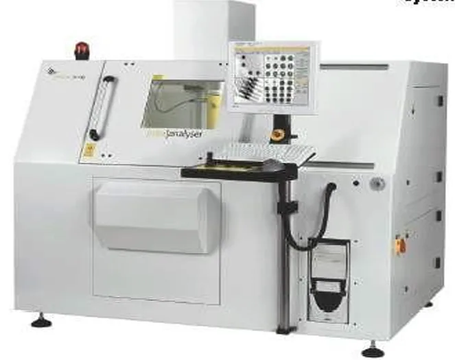
- X-Ray (AXI): Penetrates PCB layers to inspect hidden solder joints, such as those under BGAs, QFNs, or LGAs.
- ICT (In-Circuit Test): Uses a "bed of nails" fixture to electrically probe individual components for resistance, capacitance, and shorts/opens.
- FCT (Functional Circuit Test): Simulates the final operating environment to verify the board performs its intended logic and power functions.
This playbook is designed for procurement leads and hardware engineers who need to balance test coverage against cost. It helps you define requirements for APTPCB (APTPCB PCB Factory) or other vendors, ensuring you pay only for the testing rigor your product class requires.
When to use each test (and when not to)
Once you understand the definitions, the next challenge is determining which combination of tests applies to your specific production volume and reliability tier.
A full pcba testing strategy: aoi xray ict fct is essential for high-reliability sectors like automotive, medical, or aerospace, but may be overkill for simple consumer prototypes.
- Use the full suite (AOI + X-Ray + ICT + FCT) when:
- Field failure costs are extremely high (e.g., medical life support, automotive safety).
- The design includes complex BGAs (requires X-Ray) and high component density (requires AOI).
- Production volumes justify the NRE (Non-Recurring Engineering) cost of ICT fixtures.
- Use a reduced strategy (AOI + X-Ray + FCT) when:
- Volumes are low to medium (under 1,000 units), making ICT fixtures too expensive.
- The board has hidden components (BGAs) requiring X-Ray, but simple logic that FCT can cover without ICT.
- Use a minimal strategy (AOI + Bench Power Up) when:
- You are in the early prototyping phase.
- Budget is the primary constraint, and you accept a higher risk of manual debugging later.
What to define (coverage, limits, reports, fixtures)
After selecting the right inspection mix, you must define the technical specifications that the manufacturer will use to execute the plan.
Clear specifications prevent ambiguity; here are the key parameters to define for a pcba testing strategy: aoi xray ict fct:
- AOI Resolution: Specify camera resolution (e.g., <10µm/pixel) for 0201 or 01005 components.
- AOI Coverage: Define critical zones (e.g., "100% inspection of all IC polarity and SMT solder fillets").
- X-Ray Void Percentage: Set the maximum allowable voiding for BGAs (typically IPC Class 2 <25% or Class 3 <20%).
- ICT Test Points: Ensure design includes test pads (min 0.8mm diameter preferred) with 100% net access if possible.
- ICT Fixture Type: Specify single-sided or double-sided fixture requirements based on test point distribution.
- FCT Pass/Fail Logic: Define exact voltage ranges, current consumption limits, and LED status outputs.
- Cycle Time: Set a target test time per unit (e.g., <60 seconds) to avoid bottling neck mass production.
- Data Logging: Require storage of test logs (serial number, pass/fail status, parametric data) for traceability.
- Retest Policy: Define how many times a board can be retested before being quarantined.
- False Call Rate: Set a target for AOI false calls (e.g., <500 ppm) to prevent operator fatigue.
Risks that cause escapes (root causes & prevention)
Even with clear specifications, specific manufacturing risks can undermine the effectiveness of your testing plan if not actively managed.
A poorly implemented pcba testing strategy: aoi xray ict fct can lead to "escapes" (bad boards passing) or "bonepiles" (good boards failing); here is how to mitigate these risks:
- Risk: Shadowing in AOI
- Cause: Tall components block the camera's view of smaller adjacent parts.
- Detection: Review AOI program during First Article Inspection (FAI).
- Prevention: Use 3D AOI systems or optimize component layout during DFM.
- Risk: BGA Head-in-Pillow (HiP)
- Cause: Poor wetting between ball and paste, often invisible to 2D X-Ray.
- Detection: Intermittent failures in FCT or field use.
- Prevention: Require 5D or oblique angle X-Ray inspection and optimize reflow profiles.
- Risk: ICT Probe Damage
- Cause: Excessive probe pressure or misalignment damages test pads or traces.
- Detection: Visual inspection of test points after testing.
- Prevention: Use strain gauge testing on the fixture and limit probe force.
- Risk: FCT False Passes
- Cause: Loose tolerance in the test script allows marginal boards to pass.
- Detection: Cpk analysis of test data.
- Prevention: Perform Gauge R&R (Repeatability and Reproducibility) studies on the test rig.
- Risk: Incomplete Test Coverage
- Cause: Relying solely on FCT leaves structural defects (like weak solder) undetected.
- Detection: Field failures due to vibration/shock.
- Prevention: Enforce the full pcba testing strategy: aoi xray ict fct loop, ensuring structural integrity (AOI/X-Ray) before electrical test.
- Risk: Firmware Version Mismatch
- Cause: FCT loads wrong firmware or tests against wrong parameters.
- Detection: Checksum verification failure.
- Prevention: Implement automated barcode scanning to select the correct test program.
Validation & acceptance (pass/fail criteria)

To ensure the risks above are controlled, you must validate the test process itself before full production begins.
Validation proves that your pcba testing strategy: aoi xray ict fct is reliable and repeatable; use these steps for acceptance:
- Objective: Verify AOI Library Accuracy
- Method: Run a "Golden Board" (known good) and a "Defect Board" (known bad) through AOI.
- Criteria: System must catch 100% of introduced defects (missing part, wrong polarity) with zero false calls on the Golden Board.
- Objective: Validate X-Ray Sensitivity
- Method: Inspect a BGA with known voids or shorts.
- Criteria: Image clarity must allow software to automatically calculate void percentage within ±2% accuracy.
- Objective: ICT Fixture Strain Analysis
- Method: Place strain gauges on the PCB during the press cycle.
- Criteria: Microstrain must remain below the PCB material's fracture limit (typically <500 µε).
- Objective: FCT Gauge R&R
- Method: Test 10 boards, 3 times each, by 3 different operators.
- Criteria: Measurement variation (GR&R) must be <10% of the tolerance band.
- Objective: Test Coverage Report
- Method: Generate a report comparing BOM components to tested nets.
- Criteria: Confirm >90% electrical node coverage (or justify exclusions).
- Objective: Cycle Time Verification
- Method: Time the end-to-end process for a batch of 50 units.
- Criteria: Average time must meet the throughput required for annual volume.
- Objective: Data Integrity Check
- Method: Trace a specific serial number in the supplier's database.
- Criteria: Full history (AOI images, ICT values, FCT result) must be retrievable in <5 minutes.
- Objective: First Article Inspection (FAI)
- Method: Full dimensional and functional check of the first 5 units.
- Criteria: 100% compliance with all drawings and test specs.
Supplier checklist (RFQ, audit, traceability)
Once you have a validation plan, use this checklist to vet suppliers and ensure they can execute your strategy.
This checklist helps you audit potential partners like APTPCB to confirm they possess the necessary hardware and processes for a complete pcba testing strategy: aoi xray ict fct.
RFQ Inputs (What you send)
- Complete BOM with approved vendor list (AVL).
- Gerber files (RS-274X) and Pick & Place (XY) data.
- Test Point location map (for ICT).
- Functional Test Procedure (step-by-step logic).
- Firmware binaries and checksums (hex/bin).
- Mechanical drawings for custom fixtures.
- Estimated Annual Usage (EAU) to amortize fixture costs.
- Acceptance Quality Limit (AQL) standards.
Capability Proof (What they provide)
- List of AOI machines (2D vs 3D capabilities).
- X-Ray machine specs (resolution for fine-pitch BGAs).
- In-house ICT fixture fabrication vs outsourced.
- Ability to build custom FCT racks/boxes.
- Experience with your specific industry (e.g., automotive, medical).
- Example of a DFM report for Testability (DFT).
Quality System & Traceability
- ISO 9001 / IATF 16949 / ISO 13485 certifications.
- MES (Manufacturing Execution System) implementation.
- Barcode/QR code tracking per PCB.
- Procedure for handling "Bonepile" (failed boards).
- Calibration records for test equipment.
- ESD control plan for the test area.
Change Control & Delivery
- Engineering Change Order (ECO) management process.
- Firmware revision control system.
- Secure storage for customer test fixtures.
- Maintenance schedule for test probes (pogo pins).
- Disaster recovery plan for test data.
Decision guidance (trade-offs and decision rules)
With a qualified supplier, the final step is making trade-off decisions based on your product's specific constraints.
Not every product needs every test; use these decision rules to tailor your pcba testing strategy: aoi xray ict fct:
- If you prioritize lowest unit cost: Choose AOI + FCT. Skip ICT to save on fixture NRE and per-unit test time, but accept higher debug time for failures.
- If you prioritize zero-defect reliability (Automotive/Medical): Choose AOI + 3D X-Ray + ICT + FCT. The redundancy ensures no escapees, even if it costs more.
- If you have high BGA counts: You must choose X-Ray. AOI cannot see beneath the package, and FCT may not catch marginal solder joints that fail later.
- If you have >5,000 units/year: Choose ICT. The upfront fixture cost ($2k-$5k) is quickly recovered by the speed and diagnostic accuracy of ICT compared to manual debugging.
- If you have frequent design changes: Avoid ICT. Every layout change requires a new fixture or expensive modification. Stick to Flying Probe or FCT.
- If you need to catch counterfeit parts: Choose Electrical Testing (ICT/FCT) + X-Ray. Visual AOI often cannot distinguish fake internal dies.
FAQ (cost, lead time, fixtures, reporting)
Refining your strategy often raises specific questions about logistics and pricing; here are the answers.
Q: How does pcba testing strategy: aoi xray ict fct cost impact the total unit price? A: Typically, a full test suite adds 5-10% to the PCBA unit cost. However, it saves significantly on RMA and field repair costs, which can be 100x higher per unit.
Q: What is the lead time for developing a custom ICT or FCT fixture? A: Fixture development usually takes 2-4 weeks. This runs parallel to PCB fabrication, so it rarely delays the final assembly if ordered early.
Q: What DFM files are required to optimize pcba testing strategy: aoi xray ict fct? A: Provide ODB++ files or Gerbers with a defined "Test Point" layer. This allows engineers to verify probe access before manufacturing begins.
Q: Can X-Ray inspection be performed on all boards in mass production? A: Yes, automated inline AXI is possible but slow. For cost efficiency, most strategies use sampling (e.g., 10%) or focus only on specific BGA regions.
Q: How do materials affect pcba testing strategy: aoi xray ict fct accuracy? A: High-reflectivity solder masks (like white) can confuse older AOI cameras. Matte finishes are preferred for optical inspection accuracy.
Q: What is the difference between ICT and Flying Probe testing? A: ICT uses a fixed "bed of nails" for speed (seconds), while Flying Probe uses moving arms (minutes). Flying Probe is better for prototypes; ICT is better for volume.
Q: How do I define acceptance criteria for pcba testing strategy: aoi xray ict fct? A: Use IPC-A-610 standards for visual/X-Ray (AOI) and a detailed "Test Specification Document" for electrical parameters (ICT/FCT).
Q: Does FCT replace the need for ICT? A: Not entirely. FCT confirms if it works, while ICT tells you why it failed (e.g., "R45 is open"). ICT speeds up repair significantly.
Related pages & tools
To further refine your quality plan, explore these specific capabilities and guidelines.
- Testing & Quality Control: An overview of the integrated quality systems used to maintain high yield.
- AOI Inspection Services: Deep dive into how optical inspection catches surface defects like tombstoning and polarity errors.
- X-Ray Inspection (AXI): Learn how X-ray verifies BGA and QFN solder joint integrity invisible to the naked eye.
- ICT (In-Circuit Test): Details on bed-of-nails testing for high-volume production efficiency.
- FCT (Functional Test): How custom functional testing simulates real-world performance before shipping.
- DFM Guidelines: Design tips to ensure your board layout supports test points and inspection access.
Request a quote (Design for Manufacturability (DFM) review + pricing)
Ready to implement a secure test plan? Connect with APTPCB to get a comprehensive DFM review and a transparent quote that includes your specific testing requirements.
To get an accurate quote, please prepare:
- Gerber Files & BOM: For base assembly pricing.
- Test Plan: Indicate if you need AOI, X-Ray, ICT, or FCT.
- Volume: EAU helps us determine if hard tooling (ICT fixtures) is cost-effective.
- Drawings: Any mechanical constraints for functional test fixtures.
Conclusion (next steps)
A well-executed pcba testing strategy: aoi xray ict fct is the difference between a reliable product launch and a costly recall. By combining the surface-level speed of AOI, the depth of X-Ray, the diagnostic precision of ICT, and the real-world validation of FCT, you create a safety net that catches defects before they leave the factory. Use the checklist and specifications in this guide to align with your supplier, ensuring your testing investment directly translates to product quality.