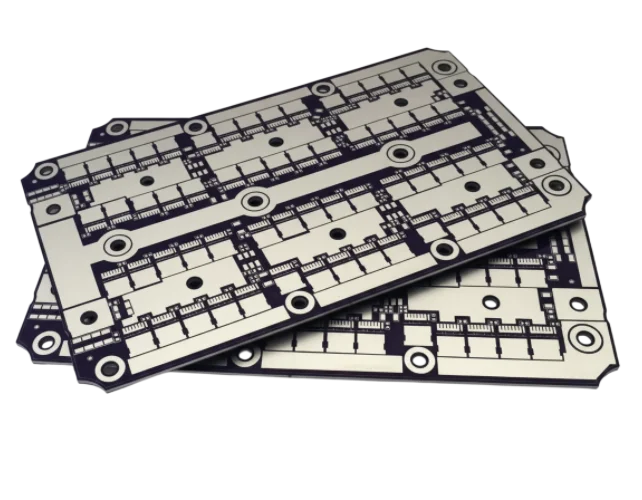
PMBus monitor PCB materials quick answer (30 seconds)
Selecting the correct PMBus monitor PCB materials is critical for ensuring signal integrity on the digital bus (SDA/SCL) and measurement accuracy on the analog sensing lines (VSENSE/ISENSE). For most industrial and server applications, the following baseline specifications apply:
- Base Material: Use High-Tg FR4 (Tg > 170°C). PMBus monitors are often placed near hot VRMs (Voltage Regulator Modules) or MOSFETs. Standard Tg (130°C) materials may soften or delaminate under continuous thermal load.
- Copper Weight: Utilize 1 oz (35µm) for signal layers to ensure fine-pitch routing of monitor ICs. Use 2 oz or higher for power planes if the PCB carries the main current, though the monitor circuit itself draws minimal power.
- Surface Finish: ENIG (Electroless Nickel Immersion Gold) is recommended. It provides a flat surface for fine-pitch PMBus controller packages (QFN/BGA) and ensures reliable contact for test points.
- Dielectric Stability: Choose materials with stable Dk (Dielectric Constant) over temperature if the design involves high-frequency switching noise coupling, though PMBus itself (400kHz/1MHz) is low speed.
- Solder Mask: High-quality LPI (Liquid Photoimageable) mask is required to prevent leakage currents between closely spaced sense lines, which can corrupt voltage readings.
APTPCB (APTPCB PCB Factory) recommends validating the Comparative Tracking Index (CTI) of the laminate if the monitor PCB operates in high-voltage environments (above 50V) to prevent tracking failures.
When PMBus monitor PCB materials applies (and when it doesn’t)
Understanding when to upgrade from standard materials to specialized PMBus monitor PCB materials ensures cost-efficiency without sacrificing reliability.
When strict material selection is required:
- Server & Data Center Power Supplies: High ambient temperatures and 24/7 operation demand High-Tg materials to prevent barrel cracking in vias.
- FPGA/ASIC Core Voltage Monitoring: When sensing sub-1V rails with millivolt accuracy, leakage through poor-quality FR4 or solder mask can skew readings.
- Automotive & Aerospace: Environments requiring wide temperature ranges (-40°C to +125°C) necessitate materials with matched CTE (Coefficient of Thermal Expansion) to prevent solder joint fatigue on sense resistors.
- High-Voltage DC-DC Converters: If the PMBus monitor crosses isolation barriers, the dielectric breakdown voltage and CTI of the material are safety-critical.
When standard materials suffice:
- Low-Power Consumer Electronics: For simple 5V/12V monitoring in room-temperature devices, standard Tg 130-140°C FR4 is sufficient.
- Prototyping & Breadboarding: Basic functionality tests do not require high-performance laminates unless thermal stress testing is involved.
- Low-Accuracy Housekeeping: If the PMBus is only used for turning rails on/off (sequencing) rather than precise telemetry, material impact is minimal.
PMBus monitor PCB materials rules and specifications (key parameters and limits)
The following table outlines the critical material parameters for a robust PMBus monitor PCB. These values help minimize thermal drift and maximize sensing accuracy.
| Rule / Parameter | Recommended Value/Range | Why it matters | How to verify | If ignored |
|---|---|---|---|---|
| Glass Transition Temp (Tg) | > 170°C (High Tg) | Prevents Z-axis expansion near hot power stages. | Check datasheet (e.g., Isola 370HR, Shengyi S1000-2). | Pad cratering or via failure during thermal cycling. |
| Decomposition Temp (Td) | > 340°C | Ensures material survives multiple reflow cycles (assembly + rework). | Review laminate Td spec. | Delamination during assembly of complex boards. |
| Copper Weight (Inner) | 1 oz (35µm) min | Provides sufficient conductivity for ground planes to shield PMBus lines. | Cross-section analysis or stackup report. | Poor noise immunity; ground bounce affecting logic levels. |
| Copper Weight (Outer) | 1 oz or 2 oz | 2 oz preferred if sense resistors carry significant current; 1 oz for fine pitch. | Specify in Gerber/Fab notes. | Overheating traces or inability to route fine-pitch ICs. |
| Surface Finish | ENIG or ENEPIG | Flatness for QFN/BGA; oxidation resistance for test points. | Visual inspection; XRF thickness measurement. | Poor solder joints on small pads; contact issues during ICT. |
| Dielectric Constant (Dk) | 3.8 – 4.5 @ 1MHz | Stable Dk helps maintain consistent impedance for noise rejection. | Impedance coupon test (TDR). | Inconsistent capacitive coupling of noise onto sense lines. |
| Loss Tangent (Df) | < 0.02 | Low loss is less critical for PMBus but indicates resin quality. | Material datasheet. | Higher risk of moisture absorption in cheap resins. |
| Moisture Absorption | < 0.3% | Moisture changes Dk and causes "popcorning" during reflow. | Pressure Cooker Test (PCT) data. | Board delamination; leakage current increases. |
| CTE (Z-axis) | < 3.0% (50-260°C) | Reduces stress on plated through-holes (PTH). | TMA (Thermal Mechanical Analysis) data. | Open circuits in vias connecting sense lines to inner layers. |
| Solder Mask Type | LPI, Halogen-free | Prevents dendritic growth and leakage between fine-pitch pins. | IPC-SM-840 qualification. | Electrochemical migration causing shorts or measurement errors. |
| Comparative Tracking Index (CTI) | PLC 3 (175V-249V) or better | Prevents carbon tracks under high voltage stress. | UL Yellow Card rating. | Electrical breakdown in high-voltage monitoring applications. |
| Peel Strength | > 1.05 N/mm | Ensures traces don't lift during rework of sense resistors. | Peel test per IPC-TM-650. | Damaged pads during component replacement. |
PMBus monitor PCB materials implementation steps (process checkpoints)
Designing a PMBus monitor PCB requires a systematic approach to material selection and layout integration. Follow these steps to ensure the physical board supports the protocol's requirements.
Define the Thermal Environment
- Action: Calculate the maximum expected temperature of the power components (MOSFETs, Inductors) adjacent to the PMBus monitor IC.
- Parameter: If T_ambient > 85°C or T_junction > 105°C, mandate High-Tg materials.
- Check: Verify the selected laminate's Tg is at least 20°C above the maximum operating temperature.
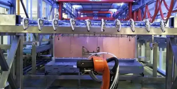
Select the Stackup and Laminate
- Action: Choose a multilayer PCB structure (4-layer minimum) to provide a dedicated ground plane.
- Parameter: Layer 2 should be a solid GND plane to shield SDA/SCL and VSENSE lines from switching noise.
- Check: Confirm with APTPCB that the chosen core and prepreg thicknesses are available in High-Tg stock.
Determine Copper Weight for Sensing Accuracy
- Action: Analyze the current sensing method (Shunt Resistor vs. DCR Sensing).
- Parameter: For shunt resistors, use Kelvin connections. If the PCB traces carry high current, use heavy copper (2 oz+) to reduce self-heating, which causes resistance drift.
- Check: Calculate voltage drop across traces; ensure it is < 0.1% of the signal for accurate telemetry.
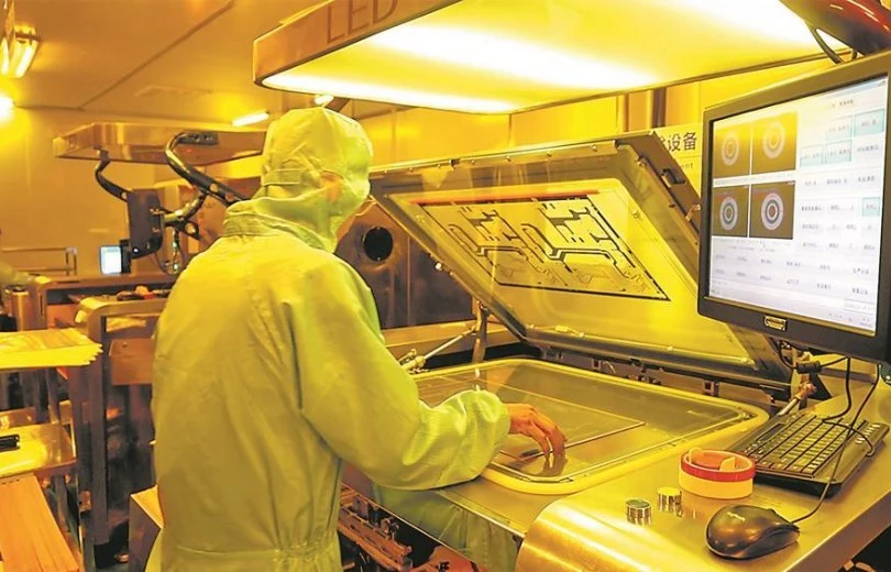
Choose the Surface Finish
- Action: Select a finish compatible with the smallest component pitch (usually the PMBus controller).
- Parameter: For 0.5mm pitch QFNs or smaller, avoid HASL (Hot Air Solder Leveling) due to unevenness. Use ENIG.
- Check: Verify the finish shelf life matches your production schedule (ENIG typically 12 months).
Optimize Solder Mask for Leakage Control
- Action: Specify high-quality LPI solder mask, especially between the differential sense pair lines.
- Parameter: Minimum solder dam width of 3-4 mils (0.075-0.1mm).
- Check: Ensure no mask openings expose bare copper near high-voltage nodes to prevent creepage.
Validate Impedance and Routing
- Action: While PMBus is not impedance-critical like PCIe, routing it as a differential pair (loose coupling) helps reject common-mode noise.
- Parameter: Trace width/spacing of 5/5 mils or 6/6 mils is standard.
- Check: Run a DFM check to ensure the selected material supports the required trace widths without over-etching.
Final Material Verification
- Action: Review the IPC-4101 specification sheet for the chosen material.
- Parameter: Look for "inorganic fillers" if thermal conductivity is a priority.
- Check: Confirm the material is RoHS compliant and UL certified.
PMBus monitor PCB materials troubleshooting (failure modes and fixes)
Improper material selection or manufacturing defects can lead to subtle failures in PMBus monitoring.
1. Intermittent Communication Loss (ACK Errors)
- Symptom: The host controller receives NACKs or corrupted data packets randomly.
- Cause: Ground bounce or noise coupling due to insufficient shielding or high-impedance return paths on thin copper.
- Check: Verify if the stackup includes a solid reference plane. Check for "woven glass effect" on very high-speed lines (less likely on PMBus, but possible on mixed-signal boards).
- Fix: Increase copper weight on ground planes; switch to a material with better resin distribution.
2. Voltage Reading Drift (Telemetry Error)
- Symptom: Reported voltage drifts over time as the board heats up.
- Cause: CTE mismatch between the sense resistor and the PCB substrate causes stress on solder joints, increasing contact resistance.
- Check: Inspect solder joints for micro-cracks. Review the CTE-Z and CTE-XY of the laminate.
- Fix: Use High-Tg PCB materials with lower Z-axis expansion. Use larger resistor packages or compliant leads.
3. PCB Discoloration or Delamination
- Symptom: Dark spots or blistering near the power stage or PMBus monitor.
- Cause: Operating temperature exceeds the material's Tg or Td.
- Check: Measure the temperature at the PCB surface during full load.
- Fix: Upgrade to a phenolic-cured FR4 or a ceramic-filled material for better thermal management.
4. Leakage Current / Phantom Voltage
- Symptom: The monitor reports a non-zero voltage when the rail is off.
- Cause: Ionic contamination trapped under the solder mask or moisture absorption in the laminate (low quality FR4).
- Check: Perform an Ion Chromatography test. Check moisture absorption specs (<0.3%).
- Fix: Improve board cleaning process; switch to materials with higher CTI and lower moisture absorption.
5. Open Vias in Sense Lines
- Symptom: Loss of VSENSE connection after thermal cycling.
- Cause: Barrel cracking due to excessive Z-axis expansion of the laminate.
- Check: Cross-section the vias.
- Fix: Use materials with lower Z-axis CTE; increase plating thickness in vias (Class 3 requirement).
PMBus monitor PCB materials: How to choose: Standard FR4 vs. High-Performance Materials
When specifying PMBus monitor PCB materials, the decision often comes down to cost versus reliability requirements.
Standard FR4 (Tg 130-140°C)
- Pros: Lowest cost, widely available, easy to process.
- Cons: High Z-axis expansion, softens at soldering temps, poor thermal conductivity.
- Best For: Consumer devices, ambient temperature operation, low current (<5A) rails, non-critical monitoring.
High-Tg FR4 (Tg 170-180°C)
- Pros: Excellent thermal stability, lower expansion, better reliability in harsh environments.
- Cons: 10-20% higher material cost than standard FR4.
- Best For: Server motherboards, industrial power supplies, automotive electronics, designs with BGA/QFN components.
Halogen-Free Materials
- Pros: Environmentally friendly, often has lower CTE and better moisture resistance.
- Cons: Can be more brittle (harder to drill), slightly higher cost.
- Best For: Green compliance markets (EU), high-reliability mobile devices.
Metal Core PCB (MCPCB)
- Pros: Superior thermal dissipation.
- Cons: Single layer limitations usually make it unsuitable for complex PMBus routing (which requires multiple signal layers).
- Best For: The power stage itself (LEDs, Power Modules), but rarely used for the complex digital monitor section unless it is a hybrid stackup.
PMBus monitor PCB materials FAQ (cost, lead time, Design for Manufacturability (DFM) files, stackup, impedance, Dielectric Constant (DK)/Loss Tangent (DF))
1. Does PMBus speed (100kHz vs 400kHz vs 1MHz) affect material choice? Generally, no. These speeds are slow enough that standard FR4 dielectric loss (Df) is not a limiting factor. However, the noise environment created by the power supply being monitored dictates the need for good ground planes and potentially higher-grade materials to maintain isolation.
2. Can I use standard FR4 for a 100A power monitor? You can use FR4, but you must manage the heat. If the copper traces heat up significantly, standard FR4 may delaminate. For high currents, prioritize heavy copper PCB specs and High-Tg laminates to withstand the thermal stress.
3. Why is ENIG preferred over HASL for PMBus monitors? PMBus monitor ICs often come in small QFN or BGA packages. HASL leaves uneven solder mounds that can cause bridging or open joints on these fine-pitch parts. ENIG provides a perfectly flat surface.
4. How does material thickness affect PMBus routing? Thinner dielectrics (prepregs) allow for closer coupling of signal traces to the reference plane, which improves noise immunity. A standard 1.6mm board is fine, but ensure the internal stackup places the PMBus signals adjacent to a ground plane.
5. Do I need "Low Dk" materials like Rogers for PMBus? No. Rogers/Teflon materials are for RF/Microwave frequencies (GHz range). Using them for PMBus is an unnecessary cost. Stick to high-quality FR4.
6. What data do I need to send for a quote? Send Gerber files, the Bill of Materials (BOM) if assembly is required, and a fabrication drawing specifying the IPC class (usually Class 2 or 3), copper weight, and material Tg requirements.
7. How do I prevent "Black Pad" on PMBus monitors? Black pad is a defect associated with ENIG. To prevent it, ensure your PCB manufacturer controls the phosphorus content in the nickel bath. Alternatively, specify ENEPIG (Electroless Nickel Electroless Palladium Immersion Gold) for higher reliability, though at a higher cost.
8. Is impedance control required for PMBus? Strict impedance control (e.g., +/- 5%) is rarely required for PMBus. However, good layout practices (differential routing, ground shielding) are essential.
9. Can I use flexible PCB materials for PMBus monitoring? Yes, Flex PCBs are common in battery management systems (BMS) where the monitor must fit into tight spaces. Use Polyimide (PI) with stiffeners under the monitor IC components.
10. What is the lead time for High-Tg PMBus boards? Standard High-Tg materials are usually in stock at APTPCB. Lead times are typically similar to standard boards (24-48 hours for prototypes), whereas exotic materials might add days.
Resources for PMBus monitor PCB materials (related pages and tools)
- High Tg PCB Manufacturing: Essential for thermal stability in power monitoring.
- Heavy Copper PCB: Required for the power rails that the PMBus system monitors.
- PCB Surface Finishes: Compare ENIG vs HASL for fine-pitch components.
- Component Sourcing: We can source PMBus controllers (TI, Analog Devices, etc.) for your assembly.
- DFM Guidelines: Design rules to ensure your board is manufacturable.
PMBus monitor PCB materials glossary (key terms)
| Term | Definition |
|---|---|
| PMBus | Power Management Bus. An open standard protocol for digital management of power supplies. |
| Tg (Glass Transition Temperature) | The temperature at which the PCB resin changes from a hard, glassy state to a soft, rubbery state. |
| CTI (Comparative Tracking Index) | A measure of the electrical breakdown (tracking) properties of an insulating material. |
| VSENSE | The voltage sensing line used by the monitor IC to measure the rail voltage. |
| Kelvin Connection | A 4-wire sensing method that eliminates the effect of trace resistance on measurement accuracy. |
| ENIG | Electroless Nickel Immersion Gold. A surface finish offering excellent flatness and oxidation resistance. |
| CTE (Coefficient of Thermal Expansion) | How much the material expands when heated. Mismatch causes stress on solder joints. |
| IPC Class 2/3 | Manufacturing standards. Class 2 is for dedicated service; Class 3 is for high-reliability/critical systems. |
| Prepreg | Fiberglass fabric impregnated with resin, used to bond core layers in a multilayer PCB. |
| DCR Sensing | Measuring current by monitoring the voltage drop across the DC resistance of an inductor. |
| SDA / SCL | Serial Data and Serial Clock lines used in I2C and PMBus communication. |
| Stackup | The arrangement of copper layers and insulating materials in a PCB. |
Request a quote for PMBus monitor PCB materials (Design for Manufacturability (DFM) review + pricing)
Ready to manufacture your power management designs? APTPCB provides comprehensive DFM reviews to ensure your material selection matches your thermal and electrical requirements.
What to include in your request:
- Gerber Files: RS-274X format preferred.
- Fab Drawing: Specify Tg > 170°C, Copper Weight (e.g., 1oz/2oz), and Surface Finish (ENIG).
- Stackup: Number of layers and desired thickness (e.g., 1.6mm).
- Quantities: Prototype (5-10 pcs) or Mass Production volume.
- Assembly Info: If PCBA is needed, include BOM and Pick & Place files.
Conclusion (next steps)
Selecting the right PMBus monitor PCB materials is a balance between thermal endurance, signal integrity, and cost. By prioritizing High-Tg laminates, appropriate copper weights for power handling, and flat surface finishes like ENIG, you ensure that your power management system delivers accurate telemetry and withstands the rigors of operation. Whether you are designing for a data center server or an industrial control unit, proper material specification is the foundation of a reliable power system.