Definition, scope, and who this guide is for
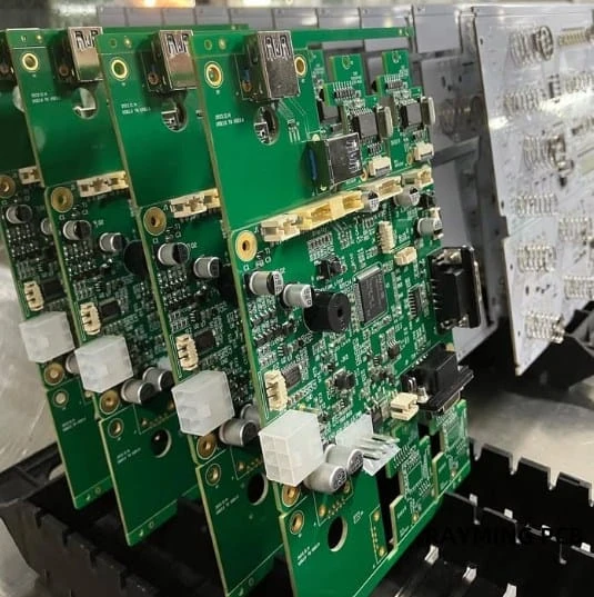
A Power Monitor PCB is a specialized circuit board designed to measure, calculate, and report electrical parameters such as voltage, current, power factor, and energy consumption. Unlike standard logic boards, these PCBs must simultaneously handle high-voltage inputs (for sensing) and low-voltage digital signals (for processing and communication) while maintaining strict isolation and thermal stability. They are the core hardware behind devices like industrial energy meters, EV charging stations, server rack PDUs, and laboratory-grade AC power analyzers.
This guide is written for hardware engineers, procurement leads, and quality managers who are responsible for sourcing reliable PCBs for power measurement applications. It moves beyond basic fabrication notes to cover the specific challenges of mixing high-current paths with precision analog sensing. You will find actionable specifications, risk mitigation strategies, and validation protocols to ensure your board performs accurately under load.
At APTPCB (APTPCB PCB Factory), we understand that a Power Monitor PCB is not just a carrier for components; it is an active element in the measurement chain. Variations in copper thickness, trace width, or material dielectric properties can directly impact measurement accuracy and safety compliance. This playbook provides the framework to define these requirements clearly to your manufacturing partner.
When to use Power Monitor PCB (and when a standard approach is better)
Building on the definition, it is critical to identify when a dedicated Power Monitor PCB design is necessary versus when a standard generic PCB layout will suffice.
Use a dedicated Power Monitor PCB approach when:
- High Accuracy is Required: Your application demands measurement accuracy better than 1% (e.g., revenue-grade metering or lab Power Analyzer PCB).
- High Voltage Isolation: The system monitors mains voltage (110V/220V/480V) and requires certified creepage and clearance distances to protect low-voltage user interfaces.
- Thermal Management: The board carries significant current (10A+) through onboard shunts or traces, requiring specific thermal dissipation strategies.
- Noise Immunity: You are measuring switching power supplies where high-frequency noise can corrupt analog signals, requiring specific stackups and shielding.
- Safety Compliance: The end product must pass UL/IEC safety standards for measurement equipment (e.g., CAT III or CAT IV ratings).
Use a standard PCB approach when:
- Indication Only: The goal is simply to detect if power is "on" or "off" without precise measurement.
- Low Voltage/Current: The system operates entirely below 50V and carries negligible current, posing no thermal or safety risks.
- External Sensors: All voltage and current sensing happens off-board (e.g., via external current transformers), and the PCB only processes digital data.
Power Monitor PCB specifications (materials, stackup, tolerances)
Once you determine that a specialized Power Monitor PCB is required, the next step is defining the engineering specifications that control performance and safety.
- Base Material (Laminate):
- Specify High Tg (Glass Transition Temperature) FR4 (Tg ≥ 170°C) to withstand thermal cycling from varying current loads without delamination.
- For high-voltage applications, request materials with a high Comparative Tracking Index (CTI), typically PLC 0 or PLC 1 (CTI ≥ 400V or 600V), to prevent tracking and arcing.
- Copper Weight:
- Standard logic areas may use 1oz copper, but current-carrying layers often require heavy copper PCB solutions (2oz, 3oz, or up to 6oz) to minimize resistance and heat rise.
- Specify the finished copper thickness explicitly (e.g., "Start 2oz, plate to 3oz") to avoid ambiguity.
- Solder Mask:
- Use high-quality, high-dielectric strength solder mask.
- Specify "Mask Dam" requirements between fine-pitch pads of high-voltage ICs to prevent solder bridging.
- Color: Green is standard, but Matte Black or White is often used for high-contrast automated optical inspection (AOI), though Green generally offers the best dam resolution.
- Surface Finish:
- Electroless Nickel Immersion Gold (ENIG) is preferred for Power Monitor PCBs. It provides a flat surface for placing fine-pitch measurement ICs and ensures reliable contact for spring-loaded test probes during calibration.
- Avoid HASL (Hot Air Solder Leveling) for precision boards as the uneven surface can cause component tilt, affecting thermal coupling.
- Layer Stackup:
- 4-layer or 6-layer designs are common to allow dedicated ground planes for noise shielding.
- Isolate high-voltage AC layers from low-voltage DC logic layers using internal prepreg layers with sufficient dielectric thickness (e.g., >0.2mm per layer for isolation).
- Trace Width and Spacing:
- Define minimum clearance based on voltage requirements (e.g., IPC-2221B standards). For 220V AC, a minimum clearance of 2.5mm might be required depending on pollution degree.
- For current sensing traces (Kelvin connections), specify matched lengths and widths to ensure differential impedance balance.
- Thermal Vias:
- Specify via-in-pad or dense thermal via arrays under heat-generating components (shunts, MOSFETs).
- Define via plugging or tenting requirements to prevent solder wicking away from the pad, which could lead to poor thermal joints.
- Dimensional Tolerances:
- Outline profile tolerance: ±0.10mm is standard, but tighter tolerances may be needed if the PCB fits into a precision machined enclosure.
- Hole size tolerance: ±0.05mm for press-fit connectors or current terminals.
- Cleanliness:
- Specify ionic contamination limits (e.g., <1.56 µg/cm² NaCl equivalent). Residues can become conductive under humidity, ruining measurement accuracy.
- Marking and Silkscreen:
- Mandate clear high-voltage warning symbols on the silkscreen.
- Ensure fuse ratings and input voltage ranges are printed clearly for service personnel.
Power Monitor PCB manufacturing risks (root causes and prevention)
Even with perfect specifications, manufacturing variations can introduce risks that compromise the safety or accuracy of a Power Logger PCB or Power Meter PCB.
- Risk: Insufficient Copper Thickness
- Root Cause: Over-etching during the manufacturing process or starting with incorrect base foil weight.
- Detection: Cross-section analysis (microsection) on coupons.
- Prevention: Specify minimum finished copper thickness in the fabrication notes, not just "nominal" weight.
- Risk: Dielectric Breakdown (Hi-Pot Failure)
- Root Cause: Voids in the FR4 material, foreign debris in prepreg, or insufficient spacing due to layer misalignment.
- Detection: Hi-Pot (High Potential) testing at the bare board level.
- Prevention: Use high-quality laminates and implement x-ray alignment checks for multilayer registration.
- Risk: Electrochemical Migration (ECM)
- Root Cause: Ionic residues left from plating or HASL flux trapped under solder mask.
- Detection: Ionic contamination testing (ROSE test).
- Prevention: Require thorough washing cycles and specify CTI-rated materials.
- Risk: Solder Mask Voiding / Peeling
- Root Cause: Poor adhesion on heavy copper traces or improper curing.
- Detection: Visual inspection and tape test.
- Prevention: Ensure the supplier uses specific mask application techniques for heavy copper (e.g., double coating or electrostatic spray).
- Risk: Inaccurate Current Sensing
- Root Cause: Variation in trace width or thickness of the shunt resistor pads/traces alters the resistance of the measurement path.
- Detection: 4-wire resistance measurement of specific test traces.
- Prevention: Tighter etching tolerances (±10% or better) for critical sensing traces.
- Risk: Thermal Delamination
- Root Cause: Trapped moisture in the PCB expanding during reflow or operation.
- Detection: Scanning Acoustic Microscopy (SAM) or blistering after reflow.
- Prevention: Bake PCBs before assembly and use high-Tg materials.
- Risk: Poor Solderability on Large Pads
- Root Cause: Large thermal mass of heavy copper pads prevents proper wetting during assembly.
- Detection: Solderability testing.
- Prevention: Design thermal relief patterns (spokes) where possible, or adjust reflow profiles.
- Risk: Creepage Distance Violation
- Root Cause: Routing errors or solder mask encroachment reducing the effective distance over the surface.
- Detection: Design Rule Check (DRC) and visual inspection.
- Prevention: Add slots (milling) between high-voltage pads to physically increase the creepage path.
- Risk: Warpage
- Root Cause: Unbalanced copper distribution between top and bottom layers.
- Detection: Bow and twist measurement.
- Prevention: Copper balancing (thieving) in the layout design phase.
- Risk: Via Cracking
- Root Cause: Z-axis expansion of the PCB material stressing the copper barrel during thermal cycling.
- Detection: Thermal shock testing followed by continuity checks.
- Prevention: Use materials with low Z-axis CTE (Coefficient of Thermal Expansion).
Power Monitor PCB validation and acceptance (tests and pass criteria)

To ensure the manufactured boards meet the rigorous demands of a Power Recorder PCB, a structured validation plan is essential.
- Objective: Verify Dielectric Strength
- Method: Perform Hi-Pot testing between high-voltage mains nets and low-voltage logic ground.
- Acceptance Criteria: No breakdown or leakage current >1mA at 2x Rated Voltage + 1000V for 60 seconds.
- Objective: Confirm Copper Thickness
- Method: Microsection analysis on a sacrificial coupon from the production panel.
- Acceptance Criteria: Measured thickness must meet the specified minimum (e.g., 65µm for 2oz finished) at the thinnest point.
- Objective: Validate Thermal Performance
- Method: Power up the PCB at maximum rated current and monitor hotspots using a thermal camera.
- Acceptance Criteria: Temperature rise must not exceed 20°C (or specified limit) above ambient at any point.
- Objective: Check Impedance/Resistance Accuracy
- Method: Precision resistance measurement of current sense traces using a micro-ohmmeter.
- Acceptance Criteria: Resistance values must fall within ±5% of the simulated design value.
- Objective: Assess Solderability
- Method: Dip and look test per IPC-J-STD-003.
- Acceptance Criteria: >95% coverage of the pad with a smooth, continuous solder coating.
- Objective: Verify Cleanliness
- Method: Ionic contamination testing (ROSE).
- Acceptance Criteria: Contamination levels <1.56 µg/cm² NaCl equivalent.
- Objective: Mechanical Dimensions
- Method: CMM (Coordinate Measuring Machine) inspection of mounting holes and outline.
- Acceptance Criteria: All dimensions within ±0.1mm tolerance.
- Objective: Plating Adhesion
- Method: Tape test on gold fingers or large pads.
- Acceptance Criteria: No metal removal or peeling.
- Objective: Thermal Shock Durability
- Method: Cycle boards between -40°C and +125°C for 100 cycles.
- Acceptance Criteria: No increase in via resistance >10% and no visible delamination.
- Objective: Visual Quality
- Method: Manual or AOI inspection at 10x magnification.
- Acceptance Criteria: No exposed copper (except pads), no bridges, no mask on pads.
Power Monitor PCB supplier qualification checklist (RFQ, audit, traceability)
When selecting a partner like APTPCB for your Power Monitor PCB, use this checklist to ensure they have the specific capabilities required for power electronics.
RFQ Inputs (What you must send)
- Gerber Files: RS-274X format, including all copper, mask, silk, and drill layers.
- Fabrication Drawing: PDF specifying materials, stackup, tolerances, and special notes.
- Netlist: IPC-356 format to ensure the electrical test matches your schematic.
- Stackup Diagram: Explicitly defining dielectric thicknesses for isolation.
- Drill Chart: Distinguishing between plated and non-plated holes.
- Panelization: If assembly is required, specify panel borders and fiducials.
- Testing Requirements: Voltage levels for Hi-Pot and impedance constraints.
- Volume: Prototype quantity vs. Mass production forecast.
- Lead Time: Desired delivery date.
- Special Processes: e.g., Edge plating, carbon ink, peelable mask.
Capability Proof (What the supplier must show)
- Heavy Copper Experience: Proven ability to etch 3oz+ copper with fine lines.
- High Voltage Certification: UL file number for the specific material stackup.
- CTI Material Stock: Availability of high-CTI laminates without long lead times.
- Thermal Management: Experience with high thermal conductivity boards or metal core PCBs.
- Controlled Impedance: Equipment to measure and certify trace impedance.
- Milling Accuracy: Capability to mill isolation slots with high precision.
Quality System & Traceability
- Certifications: ISO 9001 is mandatory; IATF 16949 is preferred for automotive power monitors.
- Material Traceability: Ability to trace every PCB back to the laminate batch.
- E-Test Records: Retention of electrical test logs for at least 2 years.
- Calibration: Regular calibration records for CMM, E-test, and impedance testers.
- NCMR Process: Clear procedure for handling Non-Conforming Material Reports.
- COC: Ability to provide a Certificate of Conformance with every shipment.
Change Control & Delivery
- PCN Policy: Commitment to notify of any process or material changes (Product Change Notification).
- Capacity: Sufficient spare capacity to handle demand surges.
- Packaging: ESD-safe, vacuum-sealed packaging with desiccant and humidity indicator cards.
- Logistics: Reliable shipping partners for international delivery.
- DFM Support: Engineering team available for pre-production design reviews.
- RMA Policy: Clear terms for returns and rework if defects are found.
How to choose Power Monitor PCB (trade-offs and decision rules)
Designing a Power Monitor PCB involves balancing cost, thermal performance, and accuracy. Here are the key trade-offs to consider.
- Heavy Copper vs. Busbars:
- If you prioritize integration and compactness: Choose Heavy Copper PCB. It keeps everything on one board but costs more per square inch.
- If you prioritize extremely high current (>100A) and low cost: Choose Busbars screwed onto a standard PCB. It handles massive current cheaply but increases assembly labor.
- FR4 vs. Metal Core (MCPCB):
- If you prioritize complex routing and multiple layers: Choose FR4. It allows for 4+ layers and dense logic routing.
- If you prioritize maximum heat dissipation for power LEDs or MOSFETs: Choose Metal Core PCB. It offers superior thermal transfer but is typically limited to 1 or 2 layers.
- Integrated Shunt vs. PCB Trace Shunt:
- If you prioritize high accuracy (<0.5%): Choose Integrated Shunt Components. They have low temperature drift but add BOM cost.
- If you prioritize low BOM cost: Choose PCB Trace Shunt. It uses a calibrated copper trace as a resistor. It is free but has a high temperature coefficient (poor accuracy over temp).
- ENIG vs. HASL Finish:
- If you prioritize flat pads for fine-pitch ICs: Choose ENIG.
- If you prioritize lowest cost for through-hole components: Choose HASL.
- 2-Layer vs. 4-Layer Stackup:
- If you prioritize noise immunity and safety: Choose 4-Layer. Internal planes shield the sensitive analog signals from high-voltage noise.
- If you prioritize lowest unit cost: Choose 2-Layer. It is cheaper but requires careful layout to avoid noise coupling.
Power Monitor PCB FAQ (cost, lead time, Design for Manufacturability (DFM) files, materials, testing)
Q: How does copper weight affect the cost of a Power Monitor PCB? A: Increasing copper weight from 1oz to 3oz can increase the bare board cost by 20-40%. This is due to the higher raw material cost of copper and the longer etching and plating cycles required in manufacturing.
Q: What is the typical lead time for a custom Power Analyzer PCB? A: Standard prototypes typically take 5-7 days. However, if you require non-standard materials (like 3oz+ copper or high-CTI FR4), lead times may extend to 10-12 days to procure the specific laminate.
Q: Do I need to provide specific DFM files for high-voltage isolation slots? A: Yes. You should clearly indicate isolation slots on the mechanical layer or outline layer of your Gerber files. Ensure the slot width is at least 0.8mm to 1.0mm to allow for standard routing bits without breakage.
Q: Can APTPCB manufacture Power Monitor PCBs with mixed copper weights? A: While "mixed copper" on the same layer is not standard, we can achieve effective heavy copper in specific areas using busbar embedding or selective plating techniques. Contact our engineering team for feasibility.
Q: What materials are best for high-voltage AC Power Analyzer PCBs? A: We recommend FR4 materials with a high Comparative Tracking Index (CTI > 600V, PLC 0). This prevents the material from becoming conductive (tracking) when exposed to high voltage and environmental contamination.
Q: How do you test the reliability of the current carrying paths? A: Beyond standard E-test, we can perform rigorous testing protocols such as 4-wire Kelvin resistance testing on specific nets to ensure the trace resistance matches your design calculations.
Q: What are the acceptance criteria for heavy copper trace width? A: Due to the side-etching effect, heavy copper traces typically have a trapezoidal shape. We generally hold a tolerance of ±20% on the top width for 3oz+ copper, compared to ±10% for standard 1oz copper.
Q: Is conformal coating necessary for Power Monitor PCBs? A: It is highly recommended. Conformal coating protects the high-voltage areas from moisture and dust, which can reduce the effective creepage distance and lead to arcing over time.
Resources for Power Monitor PCB (related pages and tools)
- Heavy Copper PCB Solutions: Explore our capabilities for manufacturing boards with up to 6oz copper, essential for handling high currents in power monitors.
- High Thermal Conductivity Boards: Learn about material options that help dissipate heat generated by shunt resistors and power components.
- DFM Guidelines for Power Electronics: Access our design for manufacturing guide to optimize your layout for production yield and cost.
- Rigorous Testing Protocols: Understand the specific validation steps we take to ensure your boards meet safety and performance standards.
Request a quote for Power Monitor PCB (Design for Manufacturability (DFM) review + pricing)
Ready to move your design to production? Request a quote today, and our engineering team will perform a comprehensive DFM review to identify potential high-voltage or thermal risks before fabrication begins.
To get the most accurate quote and DFM feedback, please provide:
- Gerber Files: Complete set including drill and mechanical layers.
- Stackup Details: Specifically mentioning dielectric thickness for isolation.
- Copper Requirements: Finished copper weight for inner and outer layers.
- Testing Specs: Any specific Hi-Pot or resistance testing requirements.
- Volume: Estimated annual usage for volume pricing.
Conclusion (next steps)
A Power Monitor PCB is the critical interface between raw electrical energy and actionable data. Whether you are building a precision Power Analyzer PCB for the lab or a rugged Power Meter PCB for the field, the reliability of your measurement depends on the quality of the board's fabrication. By defining clear specifications for materials, copper weight, and isolation, and by partnering with a manufacturer that understands the nuances of power electronics, you can ensure your product delivers accurate, safe, and consistent performance.