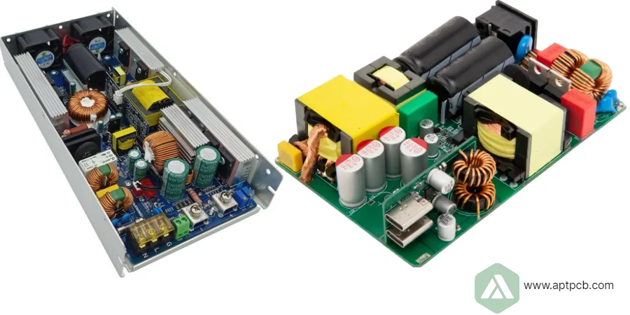
Power supply PCBs convert and regulate electrical power across consumer electronics, industrial equipment, telecommunications infrastructure, medical devices, and computing systems requiring high efficiency (>90%), electromagnetic compatibility meeting international standards, and reliable operation supporting 50,000-100,000+ hour lifetimes across diverse input voltages, output configurations, and environmental conditions ranging from -40°C arctic installations through +85°C industrial enclosures.
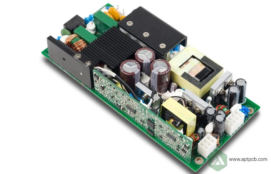
At APTPCB, we manufacture power supply PCBs implementing optimized layouts for switching converters, linear regulators, and isolated topologies across power ranges from <1W USB chargers through multi-kilowatt server and industrial supplies. Our manufacturing expertise includes EMI filtering integration, thermal management optimization, and comprehensive compliance testing supporting UL, CE, and regional safety certifications.
Implementing Efficient Power Conversion Topologies
Modern switching power supplies achieve 85-95% efficiency through advanced topologies including flyback, forward, half-bridge, full-bridge, and resonant converters selected based on power level, isolation requirements, and cost constraints. Topology selection influences component stress, electromagnetic interference, efficiency curve shape, and transient response requiring careful trade-off analysis balancing performance, cost, and reliability.
At APTPCB, our PCB manufacturing supports diverse power supply topologies with optimized layouts.
Key Topology Implementation
Flyback Converter Integration
- Single-switch topology (10-150W) minimizing component count and cost for space-constrained applications
- Transformer design integrating magnetizing inductance eliminating separate output inductor
- Discontinuous or continuous conduction mode operation optimizing efficiency across load ranges
- Clamp circuits limiting voltage spikes across switch protecting MOSFET from overvoltage
- PCB layout minimizing switching loop area reducing EMI generation and voltage ringing
- Multiple output capability deriving auxiliary voltages from single transformer core
Forward and Half-Bridge Designs
- Higher power capability (100-500W) using transformer reset mechanisms preventing core saturation
- Reduced switch voltage stress enabling lower Rds(on) MOSFETs improving efficiency
- Synchronous rectification on outputs eliminating diode losses improving low-voltage output efficiency
- EMI filter integration managing conducted and radiated emissions meeting standards
- Thermal management distributing losses across multiple components preventing hot spots
- Component placement following manufacturer guidelines optimizing magnetic coupling and minimizing parasitics
Resonant Converter Implementation
- Soft-switching topologies (LLC, LCC) achieving >95% efficiency through zero-voltage or zero-current switching
- Operating at resonant frequency minimizing switching losses and enabling higher switching frequencies
- Reduced EMI generation from sinusoidal waveforms compared to hard-switched square waves
- Wide input range capability maintaining regulation despite AC input variations or battery discharge
- Magnetics integration requiring custom transformer designs optimizing leakage inductance
- Digital control implementation enabling adaptive operation across varying load and input conditions
Linear Regulator Applications
- Low-noise regulation (<10μV RMS) for analog and RF circuits requiring clean power
- Simple implementation using LDO regulators achieving fast transient response
- Thermal management critical due to power dissipation proportional to voltage drop
- Post-regulation cleaning switching converter outputs removing residual ripple
- Multiple output voltages derived from single input minimizing supply count
- Compact PCB layouts leveraging integrated solutions for space-constrained applications
Topology-Optimized Manufacturing
Through expertise across diverse power topologies, optimized PCB layouts, and validated component selection, APTPCB enables power supply manufacturers achieving efficiency, cost, and performance targets across consumer, industrial, and telecommunications markets.
Managing Thermal Challenges and Heat Dissipation
Power supplies dissipate 5-15% of throughput power as heat requiring effective thermal management maintaining semiconductor junction temperatures below 125-150°C specifications, electrolytic capacitor temperatures below 85-105°C ratings, and magnetic cores below 100-130°C preventing excessive losses. Inadequate thermal design causes immediate failures from thermal shutdown, accelerated aging reducing lifetime, or catastrophic destruction from thermal runaway particularly in electrolytic capacitors.
APTPCB implements comprehensive thermal strategies ensuring reliable continuous operation.
Key Thermal Management Techniques
Power Semiconductor Thermal Design
- Heat sink interface design minimizing thermal resistance between packages and heat sinks
- Thermal interface materials selection achieving <0.5°C/W resistance
- PCB copper distribution spreading heat from power components across board area
- Thermal via arrays conducting heat through PCB layers to opposite-side cooling
- Package selection prioritizing exposed pad designs maximizing heat extraction
- Component placement considering airflow patterns optimizing convective cooling
Magnetic Component Thermal Management
- Core material selection balancing frequency response, saturation, and loss characteristics
- Winding design minimizing AC resistance and proximity effect losses
- Adequate spacing between transformers and heat-generating components preventing thermal coupling
- Potting or encapsulation improving heat transfer while providing mechanical support
- Temperature monitoring using thermistors or sensors enabling protection and diagnostics
- Thermal testing validating core temperatures remain within material specifications
PCB Thermal Design
- Heavy copper layers (2-4oz) in power distribution paths reducing resistive heating
- Copper pour areas beneath components spreading heat improving thermal distribution
- Multi-layer construction with internal power planes providing heat spreading
- Thermal relief connections balancing thermal performance against solderability
- Material selection considering thermal conductivity requirements for high-power applications
- Thermal simulation predicting temperatures validating designs before prototyping
Cooling System Integration
- Natural convection designs optimizing board orientation and component placement
- Forced air cooling using fans sized for required airflow at acceptable noise levels
- Heat sink selection balancing thermal performance, cost, weight, and mounting complexity
- Liquid cooling for highest power density applications using cold plates or heat pipes
- Environmental considerations accounting for altitude, ambient temperature, and dust
- Production testing measuring temperatures under rated load conditions validating thermal performance
Thermally Robust Power Supplies
By integrating thermal analysis, validated heat sink designs, and comprehensive thermal testing, APTPCB delivers power supply PCBs maintaining safe operating temperatures throughout extended service lives supporting reliable operation across diverse applications and environments.
Ensuring EMC Compliance and Safety Standards
Power supplies generate electromagnetic interference from high-speed switching requiring comprehensive EMC design achieving compliance with conducted emissions (EN 55022, FCC Part 15), radiated emissions, and immunity requirements. Safety standards (UL, VDE, IEC 60950, IEC 62368) mandate isolation barriers, creepage distances, and protection circuits ensuring user safety despite single-fault conditions. Non-compliant designs fail regulatory testing requiring expensive redesign delaying market introduction.
APTPCB implements EMC and safety compliance strategies throughout manufacturing.
Key Compliance Requirements
Conducted EMI Management
- Input filter design using common-mode and differential-mode filtering meeting emission limits
- Component selection balancing filtering performance against inrush current and leakage current
- X and Y capacitor sizing achieving noise attenuation while meeting safety requirements
- Filter layout minimizing parasitic inductance and ensuring proper grounding
- Common-mode choke design with adequate core material and winding configuration
- Pre-compliance testing during development identifying issues before formal certification testing
Radiated EMI Control
- PCB layout minimizing switching loop areas reducing magnetic field emissions
- Shielding enclosures with proper gaskets and filtered connectors maintaining barrier integrity
- Switching frequency selection avoiding problematic frequency bands when possible
- Edge rate control slowing transitions reducing high-frequency spectral content
- Cable management using shielded cables or proper twisted-pair routing
- Antenna mode reduction through balanced layout and proper grounding
Safety Isolation Implementation
- Reinforced isolation between primary and secondary maintaining >4kV barriers
- Creepage and clearance distances per safety standards (typically 6-8mm for reinforced isolation)
- High-voltage PCB materials with enhanced tracking resistance
- Isolation testing including hipot and partial discharge validation
- Protective earth connection and grounding strategy ensuring safe fault handling
- Secondary circuit protection preventing hazardous voltages despite primary circuit failures
Supporting Multiple Output Configurations
Many applications require multiple output voltages powering diverse circuits: microcontrollers (3.3V, 5V), analog circuits (±12V, ±15V), motor drives (24V, 48V), and peripherals (USB 5V). Multi-output supplies derive voltages from single converter using multiple secondary windings, post-regulators, or isolated DC-DC modules. Implementation choices influence cross-regulation, holdup time, transient response, and cost requiring optimization for specific applications.
APTPCB manufactures multi-output power supply PCBs with validated performance.
Key Multi-Output Implementation
Multiple Secondary Winding Configuration
- Transformer design with multiple secondary windings providing isolated or referenced outputs
- Winding coupling optimization balancing cross-regulation against leakage inductance
- Regulation strategy selecting primary or secondary side control determining cross-regulation performance
- Output filtering and rectification optimizing each output independently
- Current sensing and protection for each output preventing single overload affecting other outputs
- PCB layout accommodating multiple rectification and filtering sections with proper spacing
Post-Regulation Options
- Linear post-regulators providing tight regulation and low noise on critical outputs
- DC-DC post-regulators improving efficiency compared to linear alternatives
- Load sharing considerations ensuring primary converter adequately sized for all outputs
- Sequencing control enabling specific power-up and power-down sequences required by processors
- Independent protection for each output preventing fault propagation between sections
- Communication interfaces monitoring and reporting status of all outputs
Enabling High-Volume Cost-Effective Production
Power supply markets demand competitive pricing while maintaining quality and reliability. Manufacturing optimization must reduce costs through material standardization, process efficiency, and supply chain management without compromising the 50,000-100,000 hour operational lifetimes required by telecommunications, industrial, and consumer applications.
APTPCB implements cost optimization strategies balanced with reliability requirements.
Key Cost Optimization Approaches
Design for Manufacturing
- Component standardization across product lines reducing inventory and improving pricing
- Common PCB platforms accommodating multiple power levels through component substitution
- Automated assembly optimization minimizing manual operations and labor costs
- Test optimization validating critical functions without excessive test time
- Supplier partnerships ensuring component availability and competitive pricing
- Volume commitments leveraging purchasing power achieving better material costs
Process Efficiency
- High-speed automated assembly equipment maximizing throughput
- Reflow profile optimization achieving reliable solder joints minimizing rework
- Inline inspection and testing detecting defects early preventing downstream waste
- Statistical process control monitoring key parameters enabling proactive quality management
- Continuous improvement programs identifying and eliminating process waste
- Flexible manufacturing cells accommodating product mix variations without excessive changeover
Through cost-conscious design, efficient manufacturing processes, and strategic supply chain management, APTPCB enables power supply manufacturers achieving competitive market pricing while maintaining the quality and reliability required for successful products across diverse markets worldwide.
Delivering Application-Specific Solutions
Power supplies serve diverse applications spanning consumer electronics (phone chargers, laptops), telecommunications (48V infrastructure, base stations), industrial (motor drives, automation), medical (patient monitoring, surgical equipment), and computing (servers, workstations) requiring application-specific optimizations in efficiency, form factor, protection features, certifications, and environmental specifications.
APTPCB provides flexible manufacturing supporting diverse application requirements through configurable designs and comprehensive engineering support.
Key Application Optimization
Consumer Electronics
- Compact size and light weight prioritizing power density and cost
- Universal input (85-265VAC) accommodating global markets without modification
- Energy efficiency standards (DOE Level VI, ErP) minimizing standby power
- USB and fast charging protocol support delivering optimal power to modern devices
- Safety certifications (UL, CE, CCC, PSE) enabling worldwide market access
- High-volume manufacturing achieving consumer electronics pricing targets
Telecommunications Infrastructure
- 48V nominal input (36-75V operating range) matching telecom industry standards
- High reliability (>99.999% uptime) through redundancy and robust design
- Wide operating temperature (-40 to +65°C) surviving outdoor and unconditioned environments
- EMI compliance ensuring coexistence with sensitive communications equipment
- Network management integration (SNMP, PMBus) enabling remote monitoring
- Long service life (15-20 years) matching infrastructure equipment lifetimes
Through application-specific optimization, flexible manufacturing capabilities, and comprehensive support services, APTPCB enables power supply manufacturers deploying reliable, efficient solutions across diverse markets worldwide.