Prepaid Meter PCB: what this playbook covers (and who it’s for)
Utility metering has evolved from simple mechanical counting to complex electronic financial transaction nodes. The Prepaid Meter PCB is the critical hardware platform that manages this transition, handling high-voltage switching, precise metrology, and secure data communication simultaneously. For procurement leads and hardware engineers, the challenge is no longer just connectivity; it is ensuring that the board can survive 10 to 15 years in harsh field environments while maintaining the integrity of billing data.
This playbook is designed for decision-makers who need to move a metering project from prototype to mass production without encountering catastrophic field failures. It moves beyond basic datasheet parameters to address the specific manufacturing realities of smart metering. We cover the non-negotiable specifications required for safety, the hidden manufacturing risks that cause latent failures, and the validation protocols necessary to approve a supplier.
You will find a detailed breakdown of material requirements, a risk mitigation strategy for common failure modes like CAF (Conductive Anodic Filament) growth, and a comprehensive supplier audit checklist. This guide assumes you are balancing cost constraints with strict utility tender requirements and need a clear path to validating a robust supply chain.
When Prepaid Meter PCB is the right approach (and when it isn’t)
Before diving into specifications, it is vital to confirm that a dedicated Prepaid Meter PCB architecture is the correct solution for your deployment scenario.
This approach is essential when:
- Revenue Protection is Critical: You require integrated tamper detection circuits (e.g., open-case detection switches or magnetic field sensors) directly on the mainboard to prevent energy theft.
- Remote Disconnect is Required: The design must support heavy-duty latching relays capable of switching 60A to 100A, requiring specific thermal management strategies on the PCB.
- Complex Billing Logic: You are deploying a Time of Use Meter or a Smart Electric Meter that requires onboard memory and processing power to calculate tariffs locally rather than just transmitting raw pulses.
- Harsh Environments: The deployment is for outdoor or semi-outdoor environments where humidity and temperature fluctuations demand specialized surface finishes and conformal coating.
This approach may be over-engineering when:
- Sub-metering only: If the device is strictly for internal monitoring behind a main utility meter, a simpler, lower-cost standard FR4 board without high-CTI materials may suffice.
- Short Lifespan IoT: If the device is a disposable sensor node with a 2-3 year life, the rigorous 15-year durability specs of a utility-grade meter are unnecessary cost drivers.
Specs & requirements (before quoting)
To get an accurate quote and a reliable product, you must define specific parameters that go beyond standard PCB fabrication notes. Utility meters operate at the intersection of high voltage and sensitive digital logic.
- Base Material (Laminate): Specify FR4 with a High Tg (Glass Transition Temperature) of ≥150°C or ≥170°C. This ensures the board maintains mechanical stability during the thermal rise caused by high current loads.
- Comparative Tracking Index (CTI): This is non-negotiable for safety. Specify PLC-3 or PLC-0 (CTI ≥ 600V). This prevents electrical breakdown and carbon tracking across the surface of the PCB under high voltage and humidity.
- Copper Weight: For the power path (current sensing and relay connections), specify 2oz or 3oz copper. Standard 1oz is often insufficient for the thermal rise limits (usually <30°C rise) allowed in metering standards.
- Surface Finish: Electroless Nickel Immersion Gold (ENIG) is preferred for flat pads (BGA/QFN) and long-term corrosion resistance. However, Lead-Free HASL is acceptable for cost reduction if the shelf life and assembly window are tightly controlled.
- Solder Mask: Specify a high-quality, plugged via process (IPC-4761 Type VI or VII) to prevent solder wicking and entrapment of flux residues, which can lead to corrosion in humid environments.
- Cleanliness Standards: Require Ionic Contamination testing results to be <1.56 µg/cm² NaCl equivalent. Residual salts are a primary cause of field failure in Smart Water Meter and electric meter electronics.
- Dimensional Stability: Tolerances on outline and mounting holes should be tight (±0.10mm) to ensure the PCB fits perfectly into the meter casing, aligning with optical ports and disconnect switches.
- Flammability Rating: UL 94 V-0 is mandatory. The PCB must self-extinguish in the event of a component failure or terminal block overheating.
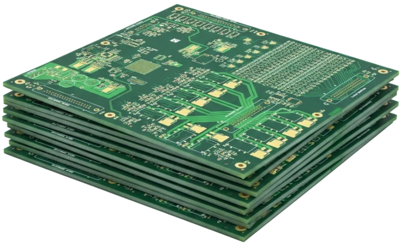
- Layer Stackup: Typically 4 layers for Smart Meter PCB designs. Layers 2 and 3 should be solid ground/power planes to shield the metrology circuits from the RF communication modules (GSM/LTE/Zigbee).
- Trace Width/Spacing: Adhere to creepage and clearance rules for the specific voltage rating (e.g., >3mm clearance for mains voltage traces).
- Marking: Silkscreen must be legible and permanent for QR codes or serial numbers used in traceability.
- Conformal Coating Readiness: If coating is applied post-assembly, the PCB fabrication drawing must specify "mask dams" or keep-out areas to prevent coating from flowing into connectors.
Hidden risks (root causes & prevention)
Scaling from a prototype to 100,000 units reveals risks that are invisible in the lab. Addressing these during the engineering phase prevents massive recalls.
Risk: CAF Growth (Conductive Anodic Filament)
- Why it happens: Electrochemical migration of copper along the glass fibers inside the PCB laminate, caused by voltage bias and humidity.
- Detection: High-voltage bias testing under humidity.
- Prevention: Use "Anti-CAF" grade laminate materials and ensure sufficient wall-to-wall distance between plated through holes (PTH).
Risk: Relay Terminal Overheating
- Why it happens: Insufficient copper volume or poor solder joints at the high-current relay connection points create resistance.
- Detection: Thermal imaging during load testing.
- Prevention: Use heavy copper (2-3oz), thermal reliefs that balance solderability with current capacity, and consider adding solder mask openings on traces to allow solder build-up (tinning) for extra conductivity.
Risk: RF Desensitization
- Why it happens: Noise from the switching power supply or metrology clock couples into the antenna path of the Smart Gas Meter or electric meter.
- Detection: Near-field scanning and receiver sensitivity testing.
- Prevention: Strict separation of analog, digital, and RF grounds. Use stitching vias to create a Faraday cage effect around sensitive RF sections.
Risk: Delamination during Assembly
- Why it happens: Moisture trapped inside the PCB expands during reflow soldering.
- Detection: Scanning Acoustic Microscopy (SAM) or cross-sectioning after reflow.
- Prevention: Enforce strict baking cycles for PCBs before assembly and store in vacuum-sealed bags with humidity indicator cards.
Risk: Plating Voids in Vias
- Why it happens: Poor drilling or plating chemistry prevents copper from fully coating the hole wall.
- Detection: Cross-section analysis and electrical continuity testing.
- Prevention: Control the aspect ratio (board thickness vs. drill diameter) and ensure the supplier uses high-throw power plating baths.
Risk: Solder Mask Peeling
- Why it happens: Poor adhesion of the mask to the copper, often due to surface contamination.
- Detection: Tape test (IPC-TM-650).
- Prevention: Ensure proper chemical cleaning and micro-etching of the copper surface before mask application.
Risk: Warpage
- Why it happens: Unbalanced copper distribution between top and bottom layers causes bowing during thermal cycles.
- Detection: Bow and twist measurement.
- Prevention: Balance copper area on opposing layers and use a symmetrical stackup.
Risk: Component Obsolescence (Design Risk)
- Why it happens: Selecting niche metrology ICs that go EOL.
- Detection: BOM scrubbing tools.
- Prevention: Design footprints that can accommodate alternative parts or use widely available standard components where possible.
Validation plan (what to test, when, and what “pass” means)

You cannot rely solely on the PCB manufacturer's final QC. You must validate the Prepaid Meter PCB at the system level.
Objective: Thermal Endurance
- Method: Temperature cycling (-40°C to +85°C) for 1000 cycles with power applied.
- Acceptance: No cracking of solder joints, no delamination, and resistance change <10%.
Objective: High Voltage Isolation
- Method: Apply 4kV impulse voltage (1.2/50µs waveform) to mains terminals.
- Acceptance: No arcing, flashover, or breakdown of the PCB insulation (CTI validation).
Objective: Humidity Resistance
- Method: Damp heat test (85°C / 85% RH) for 500 or 1000 hours.
- Acceptance: No corrosion, CAF growth, or significant drop in insulation resistance.
Objective: Vibration and Shock
- Method: Random vibration testing simulating transport and installation handling.
- Acceptance: No mechanical breakage of components or PCB traces; meter remains functional.
Objective: Solderability
- Method: Dip and look test or wetting balance test on incoming bare boards.
- Acceptance: >95% wetting coverage on pads.
Objective: Current Carrying Capacity
- Method: Inject maximum rated current (e.g., 60A) + 20% overload for 4 hours.
- Acceptance: Temperature rise of tracks must remain within safety limits (typically <30°C rise).
Objective: Electromagnetic Compatibility (EMC)
- Method: ESD testing (Contact 8kV, Air 15kV) and Radiated Immunity.
- Acceptance: Meter does not reset, hang, or corrupt memory data.
Objective: Dimensional Verification
- Method: CMM (Coordinate Measuring Machine) check of mounting holes and critical component locations.
- Acceptance: All dimensions within ±0.1mm tolerance.
Objective: Coating Adhesion (if applicable)
- Method: Cross-hatch tape test on conformal coated samples.
- Acceptance: No peeling of the coating.
Objective: Plating Thickness Verification
- Method: X-Ray Fluorescence (XRF) measurement.
- Acceptance: Gold/Nickel or Tin thickness meets IPC specifications.
Supplier checklist (RFQ + audit questions)
Use this checklist to vet potential partners like APTPCB (APTPCB PCB Factory) or others. A "yes" to these questions indicates a mature process suitable for utility metering.
RFQ Inputs (What you send)
- Complete Gerber files (RS-274X or X2).
- Fabrication drawing with material specs (Tg, CTI, Copper Weight).
- Netlist (IPC-356) for electrical test verification.
- Panelization requirements (array drawing for assembly efficiency).
- Impedance control table (if RF/High-speed signals exist).
- Surface finish and solder mask color requirements.
- Drill chart with tolerance specifications.
- Special requirements (e.g., peelable mask, carbon ink, edge plating).
- Volume projections (EAU) and batch sizes.
- Packaging requirements (vacuum pack, desiccant, humidity indicator).
Capability Proof (What they show)
- Can they demonstrate CTI ≥ 600V laminate sourcing and verification?
- Do they have experience with heavy copper (3oz+) etching?
- Can they achieve the required aspect ratio for plating?
- Do they have in-house impedance testing coupons and reports?
- Can they provide samples of similar high-voltage PCBs?
- Do they have automated optical inspection (AOI) for inner layers?
- Is their registration accuracy sufficient for the design density?
- Do they offer Design for Manufacturing (DFM) feedback?
Quality System & Traceability
- Is the facility ISO 9001 and ISO 14001 certified?
- Do they have UL certification for the specific stackup/material combo?
- Is there a system to trace raw materials (laminate, foil) to specific batches?
- Do they perform 100% electrical testing (Flying Probe or Bed of Nails)?
- Are micro-sections performed on every production panel?
- Is there a clear Non-Conforming Material (NCM) process?
- Do they use Statistical Process Control (SPC) for critical parameters?
- Are calibration records for test equipment up to date?
Change Control & Delivery
- Will they sign a Process Change Notification (PCN) agreement?
- Do they have a disaster recovery plan?
- What is their standard lead time for NPI vs. Mass Production?
- Do they have buffer stock agreements for raw materials?
- How do they handle date codes and FIFO (First In, First Out)?
- Is there a dedicated program manager for the account?
Decision guidance (trade-offs you can actually choose)
Engineering is about compromise. Here is how to navigate the trade-offs in Prepaid Meter PCB design.
Heavy Copper vs. Busbars:
- If you prioritize integration and assembly speed: Choose Heavy Copper PCB (3-4oz). It eliminates manual soldering of external busbars but increases PCB cost and etching tolerance requirements.
- If you prioritize PCB cost: Use standard 1oz copper and solder external copper busbars or shunts for the high-current path.
ENIG vs. HASL:
- If you prioritize reliability and flatness: Choose ENIG. It is essential for fine-pitch components and offers better corrosion resistance.
- If you prioritize lowest unit cost: Choose Lead-Free HASL. It is cheaper but less flat, which can be an issue for small QFNs or BGAs.
4-Layer vs. 2-Layer:
- If you prioritize EMC and RF performance: Choose a 4-Layer Stackup. Dedicated ground and power planes significantly reduce noise and improve radio range.
- If you prioritize absolute lowest cost: Choose a 2-Layer Board. This is harder to design for EMC and may require more shielding cans, potentially offsetting the savings.
High Tg vs. Standard Tg:
- If you prioritize longevity and thermal stress: Choose High Tg (170°C). It withstands the heat from relays and terminal blocks better over 15 years.
- If you prioritize material availability: Standard Tg (130-140°C) is easier to source but risky for high-current meters.
Onshore vs. Offshore Manufacturing:
- If you prioritize speed and IP protection: Prototype locally.
- If you prioritize volume cost: Move to a verified offshore partner like APTPCB for mass production once the design is frozen.
FAQ
Q: What is the most common cause of PCB failure in smart meters? A: Electrochemical migration (dendrite growth) due to moisture ingress and voltage bias. This is why CTI rating and cleanliness are critical.
Q: Why is CTI 600V (PLC-0) recommended for meter PCBs? A: Meters are often installed in uncontrolled environments (Category III or IV overvoltage). High CTI materials resist carbon tracking during voltage spikes, preventing fire hazards.
Q: Can I use a standard FR4 for a smart water meter? A: Yes, but ensure it is High Tg if the environment is hot, and prioritize moisture protection (conformal coating) as water meters are often in damp pits.
Q: How thick should the copper be for a 60A meter? A: Typically, 2oz to 3oz copper is a starting point, often supplemented by solder on exposed traces or wide track widths to manage the thermal rise.
Q: Do I need impedance control for a prepaid meter? A: Yes, if the meter uses cellular (GSM/LTE) or RF mesh communication. The antenna trace usually requires 50-ohm impedance matching.
Q: What is the lifespan of a Prepaid Meter PCB? A: Utility tenders typically demand a 15 to 20-year design life. The PCB must not degrade (delaminate or corrode) over this period.
Q: How do I prevent tampering via the PCB? A: Use internal layers for sensitive signals, add mesh ground planes to detect drilling, and include footprint pads for case-open switches.
Q: Is conformal coating mandatory? A: For outdoor or semi-outdoor meters, yes. It protects against humidity, dust, and insects which can cause short circuits.
Related pages & tools
- Power & Energy PCB Solutions – Explore specific capabilities for the energy sector, including high-voltage and high-current board manufacturing.
- Heavy Copper PCB Manufacturing – Understand the technical details of producing 3oz+ copper boards essential for handling meter load currents.
- PCB Quality Control Systems – Review the testing protocols (AOI, E-Test, Micro-sectioning) that ensure zero-defect delivery for mass production.
- Conformal Coating Services – Learn about the protective coatings applied during assembly to safeguard meters against humidity and harsh environments.
- High Tg PCB Materials – Details on high glass transition temperature materials that provide the thermal stability required for long-life utility meters.
Request a quote
Ready to validate your design for mass production? Contact APTPCB for a Quote and receive a comprehensive DFM review alongside your pricing.
To get the most accurate DFM feedback, please include:
- Gerber Files: RS-274X or X2 format.
- Fabrication Drawing: Clearly stating CTI, Tg, and Copper Weight requirements.
- Stackup Details: Layer order and dielectric thickness preferences.
- Volume: Estimated Annual Usage (EAU) to optimize panel utilization.
- Test Requirements: Specific voltage or impedance testing needs.
Conclusion
The Prepaid Meter PCB is a high-stakes component where the cost of failure far exceeds the cost of the board itself. By strictly defining material properties like CTI and Tg, understanding the hidden risks of electrochemical migration, and enforcing a rigorous validation plan, you can secure a supply chain capable of delivering utility-grade reliability. Whether you are building a Smart Electric Meter or a Time of Use Meter, the key to success lies in partnering with a manufacturer that treats your specifications as mandatory safety rules, not just suggestions.