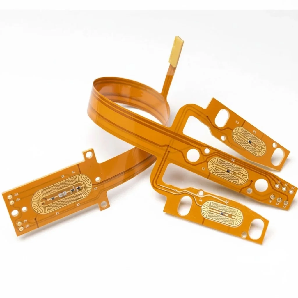
Selecting the correct PROFINET control PCB materials is the foundation of a reliable industrial automation network. Unlike standard office Ethernet, PROFINET hardware must endure harsh thermal cycles, vibration, and electromagnetic interference while maintaining precise signal integrity for real-time data transmission. Engineers often face challenges balancing cost with the strict impedance requirements needed for 100 Mbps or Gigabit communication. APTPCB (APTPCB PCB Factory) specializes in fabricating high-reliability boards that meet these stringent industrial standards. This guide details the material specifications, design rules, and troubleshooting steps necessary to ensure your PROFINET hardware performs without failure.
PROFINET control PCB materials quick answer (30 seconds)
- Dielectric Constant (Dk) Stability: Material Dk must remain stable across the operating frequency range to maintain 100Ω ±10% differential impedance.
- Thermal Reliability (Tg): Use High-Tg FR-4 (Tg > 170°C) for environments exceeding 50°C ambient or for lead-free soldering processes to prevent barrel cracking.
- Fiber Weave Effect: For Gigabit PROFINET, select "spread glass" styles (e.g., 1067, 1086) to minimize skew caused by fiber gaps.
- Moisture Absorption: Select materials with <0.3% moisture absorption to prevent delamination and impedance drift in humid factory settings.
- CAF Resistance: Conductive Anodic Filament (CAF) resistant materials are mandatory for high-density designs operating under high voltage or humidity.
- Copper Profile: Use low-profile or very-low-profile (VLP) copper foil to reduce skin effect losses in high-speed PROFINET IRT (Isochronous Real-Time) applications.
When PROFINET control PCB materials applies (and when it doesn’t)
Understanding when to upgrade from standard materials to specialized PROFINET control PCB materials prevents over-engineering or field failures.
When specialized materials are required:
- Industrial Environments: The device operates in factories with high EMI, vibration, or temperature fluctuations (-40°C to +85°C).
- Real-Time Communication (IRT): The application requires isochronous real-time data transfer where jitter and latency must be minimized.
- High Voltage Proximity: The PCB carries both low-voltage logic and high-voltage motor control power, requiring high CTI (Comparative Tracking Index) materials.
- Long Cable Runs: The PCB interfaces with long external cables, requiring robust impedance matching to prevent signal reflection.
- Multi-layer Stackups: Designs with 6+ layers requiring tight coupling between signal and ground planes.
When standard FR-4 is sufficient:
- Controlled Office Environments: The device is a simple gateway located in a climate-controlled server room.
- Low Speed/Non-Critical Data: The application uses PROFINET only for non-real-time configuration data or diagnostics.
- Short Trace Lengths: Signal traces are extremely short (<10mm) and connect directly to a pre-certified module.
- Prototypes: Initial functional testing where thermal reliability and long-term signal integrity are not yet critical.
PROFINET control PCB materials rules and specifications (key parameters and limits)
The following table outlines the critical parameters for PROFINET control PCB materials. Adhering to these limits ensures compliance with IEC 61158 and IEC 61784 standards.
| Rule / Parameter | Recommended Value/Range | Why it matters | How to verify | If ignored |
|---|---|---|---|---|
| Glass Transition Temp (Tg) | > 170°C (High Tg) | Prevents Z-axis expansion during soldering and operation. | Check datasheet (DSC method). | Plated through-hole (PTH) barrel cracks; open circuits. |
| Decomposition Temp (Td) | > 340°C | Ensures material survives multiple reflow cycles. | TGA analysis data. | Delamination during assembly or rework. |
| Dielectric Constant (Dk) | 3.8 – 4.5 (Stable) | Determines trace width for 100Ω impedance. | Impedance control calculator & TDR test. | Signal reflections; communication errors. |
| Dissipation Factor (Df) | < 0.02 @ 1GHz | Minimizes signal attenuation over long traces. | Material datasheet. | Signal loss; reduced cable reach. |
| Impedance Tolerance | 100Ω ± 10% | Critical for differential pair signal integrity. | TDR (Time Domain Reflectometry) coupons. | Packet loss; CRC errors; link drops. |
| CTE (Z-axis) | < 3.0% (50-260°C) | Reduces stress on vias during thermal cycling. | TMA method data. | Via failure in harsh thermal environments. |
| Moisture Absorption | < 0.30% | Prevents "popcorning" and electrical leakage. | IPC-TM-650 2.6.2.1. | Board delamination; impedance changes in humidity. |
| Comparative Tracking Index (CTI) | PLC 0 or 1 (>400V) | Prevents electrical breakdown between high voltage tracks. | UL 746A testing. | Arcing; short circuits in high-power zones. |
| Copper Foil Roughness | VLP or HVLP | Reduces skin effect loss at high frequencies. | SEM analysis or spec sheet. | Increased insertion loss; signal degradation. |
| Peel Strength | > 1.05 N/mm | Ensures pads do not lift during vibration or rework. | IPC-TM-650 2.4.8. | Pad lifting; component detachment. |
| Halogen Content | Halogen-Free (Optional) | Required for certain environmental compliance (RoHS/REACH). | Chemical analysis. | Non-compliance with specific EU markets. |
| CAF Resistance | Required | Prevents internal shorts along glass fibers. | IPC-TM-650 2.6.25. | Catastrophic short circuits in field. |
PROFINET control PCB materials implementation steps (process checkpoints)
Implementing the correct PROFINET control PCB materials requires a disciplined design and manufacturing process. Follow these steps to ensure the final product meets industrial standards.
Define the Stack-up and Impedance Profile
- Action: Determine layer count and select core/prepreg thicknesses to achieve 100Ω differential impedance for TX/RX pairs.
- Key Parameter: Trace width and spacing relative to reference planes.
- Acceptance Check: Simulation confirms 100Ω ±10% with selected material Dk.
- Resource: Consult PCB stack-up design guidelines.
Select the Core Material
- Action: Choose a High-Tg FR-4 laminate (e.g., Isola 370HR or equivalent) validated for industrial use.
- Key Parameter: Tg > 170°C, CAF resistant.
- Acceptance Check: Material datasheet confirms specifications match environmental requirements.
Optimize Glass Weave Selection
- Action: Specify "spread glass" or mechanically spread weave styles (1067, 1078, 1086) for high-speed signal layers.
- Key Parameter: Glass style.
- Acceptance Check: Fabrication notes explicitly state acceptable glass styles to prevent fiber weave skew.
Route Differential Pairs
- Action: Route PROFINET pairs (TX+, TX-, RX+, RX-) with strict length matching and constant spacing.
- Key Parameter: Intra-pair skew < 5 mils (0.127 mm).
- Acceptance Check: DRC (Design Rule Check) passes with no phase violations.
Implement Reference Planes
- Action: Ensure solid ground planes immediately adjacent to signal layers; do not route over splits.
- Key Parameter: Return path continuity.
- Acceptance Check: Visual inspection of Gerber files shows no voids under high-speed traces.
Specify Surface Finish
- Action: Select ENIG (Electroless Nickel Immersion Gold) for flat pads and reliable soldering of fine-pitch PHY components.
- Key Parameter: Surface flatness.
- Acceptance Check: Finish thickness specification (e.g., Au 2-5µin, Ni 120-240µin).
Verify with DFM Review
- Action: Send data to APTPCB for a Design for Manufacturability review before production.
- Key Parameter: Minimum trace/space, drill aspect ratio.
- Acceptance Check: Manufacturer confirms stack-up and material availability.
Fabrication and TDR Testing
- Action: Manufacture the PCB with impedance coupons.
- Key Parameter: TDR measurement results.
- Acceptance Check: TDR report shows impedance within 90Ω–110Ω range.
PROFINET control PCB materials troubleshooting (failure modes and fixes)
Even with the right design, issues can arise if PROFINET control PCB materials are processed incorrectly or subjected to unexpected stress.
1. Symptom: Intermittent Link Loss (Flapping)
- Causes: Impedance mismatch causing signal reflection; poor connector soldering.
- Checks: Review TDR reports; inspect RJ45/M12 connector solder joints (X-ray if needed).
- Fix: Respin with corrected stack-up for 100Ω; switch to tighter tolerance materials.
- Prevention: Use controlled impedance coupons on every panel.
2. Symptom: High Bit Error Rate (BER) or CRC Errors
- Causes: Fiber weave skew (signal travels faster on resin than glass); external EMI coupling.
- Checks: Verify glass style used; check shielding can grounding.
- Fix: Rotate design 10 degrees on panel (zigzag routing) or use spread glass.
- Prevention: Specify spread glass (e.g., 1067) in fabrication notes.
3. Symptom: Board Delamination after Reflow
- Causes: Trapped moisture in material; Td too low for lead-free profile.
- Checks: Check baking logs; verify material Td > 340°C.
- Fix: Bake boards before assembly; upgrade to higher Td material.
- Prevention: Enforce strict moisture sensitivity level (MSL) controls and vacuum packaging.
4. Symptom: Barrel Cracks in Vias
- Causes: High Z-axis expansion (CTE) during thermal cycling.
- Checks: Microsection analysis of failed vias.
- Fix: Switch to material with lower Z-axis CTE; increase plating thickness.
- Prevention: Use High-Tg materials (>170°C) for industrial temperature ranges.
5. Symptom: Conductive Anodic Filament (CAF) Shorts
- Causes: Electrochemical migration along glass fibers under voltage and humidity.
- Checks: Insulation resistance testing; look for internal shorts between power/ground.
- Fix: Scrappage required; switch to CAF-resistant resin systems.
- Prevention: Specify "CAF Resistant" laminate in material requirements.
6. Symptom: Signal Attenuation over Distance
- Causes: High Dissipation Factor (Df) or rough copper foil.
- Checks: Measure insertion loss; check copper profile specs.
- Fix: Use lower loss material or VLP (Very Low Profile) copper.
- Prevention: Calculate total loss budget including PCB traces and cabling.
How to choose PROFINET control PCB materials (design decisions and trade-offs)
Choosing the right PROFINET control PCB materials involves balancing performance against cost and manufacturability.
Standard FR-4 vs. High-Tg FR-4
- Standard FR-4 (Tg 130-140°C): Suitable for benign environments and consumer-grade electronics. Low cost. Not recommended for industrial PROFINET due to lower thermal reliability.
- High-Tg FR-4 (Tg 170°C+): The standard for industrial control PCB solutions. Offers better mechanical stability, CAF resistance, and thermal endurance. Slightly higher cost but prevents field failures.
Standard Copper vs. VLP Copper
- Standard Electrodeposited (ED): Higher surface roughness. Acceptable for 100 Mbps PROFINET.
- VLP (Very Low Profile): Smoother surface. Recommended for Gigabit PROFINET to reduce skin effect losses and improve signal integrity.
Filled vs. Unfilled Vias
- Unfilled: Standard process. Risk of solder thieving if placed in pads.
- Filled & Capped (VIPPO): Essential for high-density BGA designs (e.g., PROFINET controller chips). Improves thermal transfer but increases cost.
Material Availability vs. Performance
- Common Stock (e.g., Isola 370HR, Shengyi S1000-2): Readily available, good balance of cost and performance.
- Specialty High-Speed (e.g., Megtron 6): Overkill for standard PROFINET unless combined with very high-speed backplane data. High cost and longer lead time.
PROFINET control PCB materials FAQ (cost, lead time, common defects, acceptance criteria, Design for Manufacturability (DFM) files)
1. How does selecting High-Tg material affect the cost of PROFINET control PCB materials? High-Tg materials typically increase the bare board cost by 10-20% compared to standard FR-4. However, this cost is negligible compared to the expense of a field failure in an industrial automation line.
2. What is the typical lead time for PROFINET control PCBs with controlled impedance? Standard lead time is 5-7 days for prototypes and 10-15 days for mass production. If specialty materials (non-stock) are required, lead times may extend to 3-4 weeks.
3. Do I need specific DFM files for PROFINET control PCB materials? Yes. You must provide Gerber files (RS-274X), a drill file, and a detailed stack-up drawing specifying the target impedance (e.g., 100Ω differential) and the specific layers to be controlled.
4. What are the acceptance criteria for impedance testing? The industry standard is ±10%. For a 100Ω target, the measured impedance on the coupon must fall between 90Ω and 110Ω. Tighter tolerances (±5%) are possible but cost more.
5. Can I use standard FR-4 for Gigabit PROFINET? It is risky. While electrically possible for short traces, standard FR-4 often lacks the consistency and thermal robustness required for industrial Gigabit applications. High-Tg material is strongly recommended.
6. How do I prevent "fiber weave effect" in my PROFINET design? Specify "spread glass" styles like 1067 or 1086 in your fabrication notes. Alternatively, route high-speed differential pairs at a slight angle (e.g., 10°) relative to the weave, though this consumes more board space.
7. What surface finish is best for PROFINET control PCB materials? ENIG (Electroless Nickel Immersion Gold) is preferred. It provides a flat surface for fine-pitch components (like Ethernet PHYs) and offers excellent corrosion resistance in harsh industrial atmospheres.
8. Is halogen-free material required for PROFINET PCBs? Not strictly for performance, but many European industrial customers require halogen-free materials for environmental compliance. Check your end-user requirements.
9. How does copper thickness affect PROFINET control PCB materials? Standard 1oz (35µm) copper is typical. However, for impedance control on outer layers, 0.5oz (18µm) is often used to allow for finer trace widths while maintaining the correct impedance profile.
10. What testing should I request from the manufacturer? Request Electrical Testing (E-Test) for opens/shorts and TDR (Time Domain Reflectometry) testing for impedance verification. A TDR report should be included with the shipment.
11. Why is CAF resistance mentioned in PROFINET specs? Industrial environments often have high humidity. CAF (Conductive Anodic Filament) growth can cause internal shorts. CAF-resistant materials prevent this electrochemical migration, ensuring long-term reliability.
12. Can APTPCB assist with stack-up design for PROFINET? Yes. APTPCB engineers can propose a valid stack-up based on your layer count and impedance requirements before you begin routing.
Resources for PROFINET control PCB materials (related pages and tools)
- High-Tg PCB manufacturing: Details on materials that withstand industrial temperatures.
- PCB stack-up design: Guidelines for arranging layers to achieve signal integrity.
- Impedance control calculator: A tool to estimate trace width and spacing for 100Ω impedance.
- Industrial control PCB solutions: Overview of capabilities for the automation sector.
- Turnkey PCB assembly: Full service from material sourcing to final assembly.
PROFINET control PCB materials glossary (key terms)
| Term | Definition | Relevance to PROFINET |
|---|---|---|
| PROFINET | Process Field Network; an industry technical standard for data communication over Industrial Ethernet. | The application requiring the specific PCB materials. |
| Impedance | The opposition to AC current flow, measured in Ohms. | Must be controlled to 100Ω for differential pairs to prevent signal reflection. |
| Differential Pair | Two complementary signals (positive and negative) used to transmit data. | The primary method of signaling in Ethernet/PROFINET to reject noise. |
| Tg (Glass Transition Temp) | The temperature at which the PCB resin turns from a hard glass to a soft state. | High Tg is crucial for industrial durability. |
| Dk (Dielectric Constant) | A measure of a material's ability to store electrical energy in an electric field. | Affects signal propagation speed and trace width calculations. |
| Df (Dissipation Factor) | A measure of the power loss in a dielectric material. | Lower Df means less signal loss, important for long traces. |
| Skew | The time difference between the arrival of signals on a differential pair. | Must be minimized to prevent data errors; affected by fiber weave. |
| CAF | Conductive Anodic Filament; electrochemical migration of copper along glass fibers. | A major failure mode in humid industrial environments. |
| EMI | Electromagnetic Interference; disturbance that affects an electrical circuit. | PROFINET PCBs need shielding and ground planes to resist factory EMI. |
| IRT | Isochronous Real-Time; a PROFINET communication class. | Requires strict hardware timing and low latency, demanding high-quality PCBs. |
| TDR | Time Domain Reflectometry; a measurement technique used to determine impedance. | The standard method for verifying PCB quality. |
| Crosstalk | Unwanted signal transfer between communication channels. | Minimized by proper spacing and material selection. |
Request a quote for PROFINET control PCB materials
Ready to manufacture your industrial controller? APTPCB provides comprehensive DFM reviews and competitive pricing for high-reliability PCBs.
To get an accurate quote and DFM analysis, please provide:
- Gerber Files: RS-274X format preferred.
- Fabrication Drawing: Include stack-up, impedance requirements (e.g., 100Ω on layers 1, 3, 6), and material specs (Tg, Halogen-free, etc.).
- Quantity: Prototype vs. Mass Production volumes.
- Assembly Needs: BOM if PCBA is required.
Conclusion (next steps)
Selecting the right PROFINET control PCB materials is not just about meeting a spec sheet; it is about ensuring the longevity and safety of industrial automation systems. By prioritizing High-Tg laminates, stable dielectric constants, and CAF resistance, engineers can eliminate common failure points like signal jitter and thermal delamination. APTPCB is equipped to handle these complex requirements, delivering boards that perform reliably in the most demanding factory environments.