Definition, scope, and who this guide is for
Redundant PSU backplane design refers to the engineering and manufacturing of the printed circuit board (PCB) that acts as the central power distribution hub in high-availability systems. Unlike standard power boards, these backplanes connect multiple power supply units (PSUs)—typically in an N+1 or N+N configuration—to the system load. They must handle high current densities, facilitate hot-swapping (replacing a power supply while the system runs), and manage critical signals for power management (PMBus) without failure. The backplane is often a single point of failure; if it fails, the redundancy of the power supplies becomes irrelevant.
This guide is written for hardware engineers, system architects, and procurement leads who are responsible for sourcing or designing these critical components. It moves beyond basic PCB layout theory into the practical realities of manufacturing, material selection, and risk mitigation. You will find actionable specifications to include in your fabrication drawings, a breakdown of manufacturing risks specific to heavy copper and thick boards, and a validation strategy to ensure your Redundant PSU backplane design survives years of 24/7 operation in data centers or industrial environments.
At APTPCB (APTPCB PCB Factory), we see many designs fail not because of electrical logic errors, but because of physical manufacturing constraints like copper etching tolerances, thermal delamination, or connector misalignment. This playbook bridges the gap between your CAD file and the factory floor, ensuring that your requirements are clear, manufacturable, and verifiable.
When to use Redundant Power Supply Unit (PSU) backplane design (and when a standard approach is better)
Deciding to implement a fully custom Redundant PSU backplane design is a significant investment in engineering time and manufacturing cost, so it is vital to confirm that your application truly requires this level of complexity before proceeding.
Use a custom Redundant PSU backplane design when:
- Uptime is Non-Negotiable: Your system powers servers, storage arrays, medical equipment, or telecom infrastructure where downtime results in significant financial loss or safety risks.
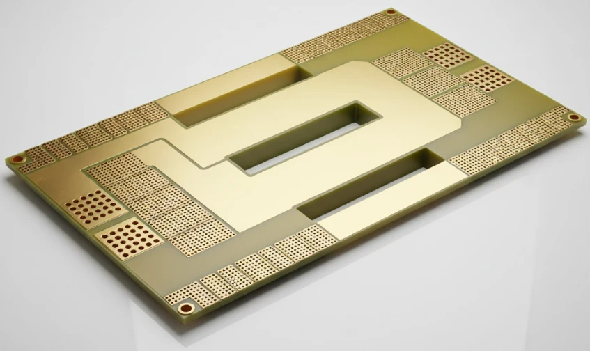
- High Current Requirements: The total system load exceeds 50A–100A, requiring heavy copper layers (3oz to 6oz) or embedded busbars that standard off-the-shelf power distribution boards cannot handle.
- Hot-Swap Capability is Required: You need precise mechanical alignment for blind-mate connectors to allow technicians to replace failed PSUs without powering down the system.
- Custom Form Factor: The power distribution must fit into a specific chassis geometry that standard ATX or OCP (Open Compute Project) power distribution boards do not fit.
- Signal Integration: You need to route low-voltage management signals (I2C, PMBus) alongside high-power rails with strict noise immunity requirements.
Stick to a standard or cable-harness approach when:
- Cost is the Primary Driver: For consumer electronics or non-critical desktop workstations, a standard single-PSU harness is significantly cheaper.
- Low Power Density: If the system draws less than 20A, standard wiring harnesses or simple 1oz copper PCBs are sufficient and easier to source.
- No Hot-Swap Needed: If the system can be powered down for maintenance, the complex mechanical tolerances of a backplane are unnecessary.
Redundant Power Supply Unit (PSU) backplane design specifications (materials, stackup, tolerances)
Defining the right specifications upfront prevents costly engineering change orders (ECOs) later. A robust Redundant PSU backplane design relies on materials that can withstand high thermal stress and mechanical loads.
Key Specifications to Define:
- Base Material (Laminate):
- Specify High Tg FR-4 (Tg ≥ 170°C) or equivalent. Power backplanes generate significant heat; standard Tg 135°C materials may delaminate over time.
- Consider CTI (Comparative Tracking Index) ≥ 600V (PLC 0) if high voltage rails (e.g., 48V or 400V DC) are present, to prevent tracking between traces.
- Copper Weight:
- Define inner and outer layer copper weight explicitly (e.g., 3oz, 4oz, or 6oz).
- Target: For currents >50A, verify trace width calculators against IPC-2152 standards, not just simple IPC-2221 formulas.
- PCB Thickness:
- Backplanes are often thicker than standard boards (2.0mm to 6.0mm) to provide mechanical rigidity for heavy connectors.
- Tolerance: Specify ±10% thickness tolerance. Tighter tolerances (±5%) may be needed for press-fit connectors.
- Layer Count & Stackup:
- Typical range: 6 to 14 layers.
- Ensure symmetrical stackup to prevent warping (bow and twist), which is critical for connector alignment.
- Dedicate specific layers for power and ground to maximize capacitance and minimize inductance.
- Surface Finish:
- Recommended: ENIG (Electroless Nickel Immersion Gold) or Hard Gold for edge fingers/contact pads.
- Avoid HASL for fine-pitch connectors or press-fit holes due to uneven surface planarity.
- Press-Fit Hole Tolerances:
- If using press-fit connectors (common in backplanes), specify finished hole size tolerances strictly (often ±0.05mm).
- Specify the drill size and plating thickness (typically min 25µm copper in barrel) to ensure a gas-tight joint.
- Soldermask:
- Use high-temperature soldermask suitable for multiple reflow cycles or wave soldering.
- Color: Matte Green or Black (Matte is better for automated optical inspection).
- Silkscreen & Marking:
- Clearly label PSU slots (PSU1, PSU2) and voltage rails (+12V, +5V, GND).
- Include high-voltage warning symbols on the silkscreen if applicable.
- Mechanical Drills:
- Specify non-plated through holes (NPTH) for guide pins with tight tolerances (+0.05mm/-0.00mm) to ensure PSUs align correctly during insertion.
- Heavy Copper Etching:
- Acknowledge minimum trace width/spacing rules for heavy copper. For 3oz copper, minimum spacing might be 8-10 mil (0.2mm-0.25mm) depending on the supplier.
Redundant Power Supply Unit (PSU) backplane design manufacturing risks (root causes and prevention)
Manufacturing a Redundant PSU backplane design introduces risks that do not exist in standard low-power PCBs. Understanding these root causes helps you audit suppliers effectively.
1. Inner Layer Misregistration
- Risk: High layer counts and thick copper can cause layers to shift during lamination.
- Root Cause: Material movement during the high-pressure press cycle.
- Prevention: Use pin-lamination techniques and include specific alignment targets (coupons) in the panel border.
2. Inufficient Resin Fill (Measling/Voids)
- Risk: Voids in the insulation between heavy copper tracks lead to shorts or dielectric breakdown.
- Root Cause: Standard prepreg sheets may not contain enough resin to fill the deep gaps between thick copper traces (e.g., 4oz copper).
- Prevention: Specify "High Resin Content" prepreg or use multiple plies of prepreg to ensure full encapsulation of heavy copper features.
3. Plated Through Hole (PTH) Cracking
- Risk: Barrel cracks disconnect power planes or signals.
- Root Cause: Z-axis expansion of the thick PCB during soldering stresses the copper barrel.
- Prevention: Ensure plating thickness meets IPC Class 3 (average 25µm). Use high Tg / low CTE (Coefficient of Thermal Expansion) materials.
4. Press-Fit Connector Damage
- Risk: PCB cracks or damaged connector pins during assembly.
- Root Cause: Incorrect hole size or insufficient PCB stiffness.
- Prevention: strict control of finished hole size (FHS) and use of a rigid support fixture during the press-fit process.
5. Thermal Management Failure
- Risk: Localized hotspots burn out the board.
- Root Cause: Poor thermal path from inner layers to the surface.
- Prevention: Use thermal vias arrays and consider Metal Core PCB technology or embedded coin technology if air cooling is insufficient.
6. Heavy Copper Undercut
- Risk: Reduced trace width increases resistance and heat.
- Root Cause: Etching chemicals eat sideways under the resist while etching down through thick copper.
- Prevention: Apply etch compensation factors in the CAM stage (design traces slightly wider) and verify final trace width with cross-section analysis.
7. Bow and Twist
- Risk: The backplane is not flat, preventing PSUs from sliding in smoothly.
- Root Cause: Asymmetrical copper distribution (e.g., Layer 1 is 90% copper, Layer 2 is 10%).
- Prevention: Balance copper coverage on all layers. Use copper pouring (thieving) in empty areas.
8. CAF (Conductive Anodic Filament) Growth
- Risk: Internal shorts develop over months of operation.
- Root Cause: Electrochemical migration along glass fibers under high voltage bias and humidity.
- Prevention: Specify "CAF-resistant" materials and maintain sufficient clearance between high-voltage nets.
Redundant Power Supply Unit (PSU) backplane design validation and acceptance (tests and pass criteria)
Validation ensures that the manufactured Redundant PSU backplane design meets the theoretical performance limits. Do not rely solely on visual inspection.

1. Electrical Continuity & Isolation (100% Test)
- Objective: Ensure no shorts or opens.
- Method: Flying probe or bed-of-nails tester.
- Criteria: 100% pass. Isolation resistance > 100 MΩ at 250V/500V.
2. Hi-Pot Testing (High Potential)
- Objective: Verify dielectric strength between power rails and chassis ground.
- Method: Apply high voltage (e.g., 1500V DC) for 60 seconds.
- Criteria: Leakage current < 1mA (or per spec); no breakdown or arcing.
3. Microsection Analysis (Coupons)
- Objective: Verify internal stackup and plating quality.
- Method: Cross-section a test coupon from the production panel.
- Criteria: Copper thickness meets spec (e.g., 3oz ±10%), hole wall plating >25µm, no resin recession or delamination.
4. Thermal Stress Test (Solder Float)
- Objective: Simulate soldering thermal shock.
- Method: Float sample in solder pot (288°C) for 10 seconds (IPC-TM-650).
- Criteria: No blistering, delamination, or lifted pads.
5. Impedance Testing (TDR)
- Objective: Verify signal integrity for PMBus/communication lines.
- Method: Time Domain Reflectometry on test coupons.
- Criteria: Measured impedance within ±10% of design target (e.g., 100Ω differential).
6. Mechanical Fit Check (First Article)
- Objective: Ensure PSUs and connectors align perfectly.
- Method: Install actual connectors and insert a dummy PSU or gauge.
- Criteria: Smooth insertion force; no binding; guide pins engage before connectors.
7. Current Carrying Capability Test (Type Test)
- Objective: Validate thermal rise under load.
- Method: Power up the backplane at max rated current and monitor temp with thermal camera.
- Criteria: Temperature rise < 30°C (or specified limit) at steady state.
8. Ionic Contamination Test
- Objective: Ensure board cleanliness to prevent corrosion.
- Method: ROSE test (Resistivity of Solvent Extract).
- Criteria: < 1.56 µg/cm² NaCl equivalent (standard IPC limit).
Redundant Power Supply Unit (PSU) backplane design supplier qualification checklist (RFQ, audit, traceability)
When selecting a partner for Redundant PSU backplane design, use this checklist to vet their capabilities. A standard PCB shop may not handle the heavy copper or strict tolerances required.
Group 1: RFQ Inputs (What you must provide)
- Gerber files (RS-274X or X2) with clear layer stackup.
- Fabrication drawing specifying IPC Class (Class 2 or 3).
- Drill chart distinguishing between plated and non-plated holes.
- Netlist (IPC-356) for electrical test verification.
- "Read Me" file detailing special requirements (e.g., "Do not X-out arrays", "Press-fit tolerances apply").
- Panelization requirements (if assembly is automated).
- Copper weight specifications for every layer.
- Impedance control table (if applicable).
Group 2: Capability Proof (What the supplier must demonstrate)
- Experience with Heavy Copper PCB manufacturing (ask for max copper weight capability).
- Ability to handle thick boards (up to 6mm or more).
- In-house press-fit connector assembly equipment (if they are doing assembly).
- UL certification (94V-0) for the specific stackup/material proposed.
- Automated Optical Inspection (AOI) calibrated for thick copper traces.
- X-Ray inspection capability for multilayer registration.
Group 3: Quality System & Traceability
- ISO 9001 certification (mandatory); IATF 16949 (preferred for high reliability).
- Material traceability: Can they trace the resin/copper lot to the specific board?
- Outgoing Quality Control (OQC) reports included with shipment.
- Cross-section reports provided for every batch.
- Calibration records for electrical testers.
- Handling procedures for moisture-sensitive devices (MSD) if assembly is involved.
Group 4: Change Control & Delivery
- PCN (Product Change Notification) policy: Do they notify you before changing material brands?
- DFM workflow: Do they provide a detailed engineering query (EQ) report before production?
- Packaging: Vacuum sealed with desiccant and humidity indicator card.
- Edge protection: Do they use protective corners for heavy backplanes during shipping?
- Lead time stability for special materials (High Tg, heavy copper).
How to choose Redundant Power Supply Unit (PSU) backplane design (trade-offs and decision rules)
Engineering is about trade-offs. Here is how to navigate the conflicting requirements in Redundant PSU backplane design.
1. Heavy Copper vs. Busbars
- If you need < 100A: Use Heavy Copper PCB (3oz–4oz). It is cost-effective and integrated.
- If you need > 150A: Consider embedded or screwed-on busbars. Etching extremely thick copper (6oz+) is expensive and limits fine pitch routing for signals.
2. High Tg FR-4 vs. Standard FR-4
- If operating temp is > 80°C or high layer count: Choose High Tg (170°C+). It reduces Z-axis expansion and barrel cracks.
- If low power/consumer grade: Standard Tg (135°C–150°C) may suffice, but the cost savings are often negligible compared to the risk.
3. Press-Fit vs. Wave Solder Connectors
- If the board is very thick (>3mm): Choose Press-Fit. Wave soldering thick boards is difficult (hole fill issues) and thermally stressful.
- If the board is standard thickness (1.6mm): Wave soldering is standard and cheaper for lower pin counts.
4. Immersion Silver vs. ENIG
- If you prioritize shelf life and contact reliability: Choose ENIG. It is robust against oxidation and excellent for press-fit.
- If you prioritize cost: Immersion Silver is cheaper but tarnishes easily if not handled correctly; generally not recommended for high-reliability backplanes.
5. Class 2 vs. Class 3 (IPC Standards)
- If "fail-safe" is the goal (Medical/Aerospace/Server): Choose IPC Class 3. It requires thicker plating and stricter defect criteria.
- If standard industrial: IPC Class 2 is usually sufficient and costs 15–20% less.
Redundant Power Supply Unit (PSU) backplane design FAQ (cost, lead time, Design for Manufacturability (DFM) files, materials, testing)
Q: How does copper weight impact the cost of Redundant PSU backplane design? A: Increasing copper weight significantly increases cost.
- Material: Heavy copper laminates are more expensive.
- Processing: Etching takes longer and depletes chemicals faster.
- Lamination: Requires more prepreg (resin) to fill gaps, adding material cost.
Q: What is the typical lead time for a custom Redundant PSU backplane? A: Expect 15–20 working days for prototypes and 20–25 days for production.
- Heavy copper and High Tg materials may have longer procurement cycles than standard FR-4.
- Complex testing (Hi-Pot, Impedance) adds 1–2 days to the process.
Q: What DFM files are critical for Redundant PSU backplane design reviews? A: Beyond Gerbers, you must provide a drill drawing with strict tolerances.
- Include a "layer map" showing exactly which layers are power planes.
- Provide the datasheet for the mating connectors so the CAM engineer can verify pad/hole dimensions.
Q: Can I use standard FR-4 for a Redundant PSU backplane design? A: It is risky.
- Standard FR-4 has a lower Tg (glass transition temperature) and higher CTE (expansion).
- Under the thermal load of redundant PSUs, standard FR-4 can soften, leading to pad cratering or barrel cracks. Always prefer High Tg materials.
Q: What are the acceptance criteria for press-fit connector holes? A: The hole tolerance is extremely tight, typically ±0.05mm (2 mil).
- The copper plating in the barrel must be smooth and continuous (min 25µm).
- The surface finish (e.g., ENIG) must not reduce the hole diameter below the connector manufacturer's minimum spec.
Q: How do you test for latent defects in Redundant PSU backplane design? A: Latent defects (like partial CAF) are hard to catch in standard E-test.
- Use IPC Class 3 plating requirements to ensure robustness.
- Perform periodic reliability testing (thermal cycling) on production samples, not just prototypes.
Q: Why is "resin starvation" a risk in Redundant PSU backplane design? A: Thick copper traces create deep "valleys" that the prepreg resin must fill during lamination.
- If the prepreg doesn't have enough resin flow, voids occur.
- Solution: Use high-flow prepreg or "double-ply" prepreg sheets between heavy copper layers.
Q: Does APTPCB support DFM for Redundant PSU backplane design? A: Yes. We perform a full DFM check on trace widths, spacing for heavy copper, and thermal management strategies before any metal is cut.
Resources for Redundant Power Supply Unit (PSU) backplane design (related pages and tools)
- Backplane PCB Manufacturing: A deep dive into the specific fabrication processes for high-layer-count backplanes.
- Heavy Copper PCB Capabilities: Essential reading for understanding the design rules and current carrying capacities of thick copper boards.
- High Tg PCB Materials: Learn why thermal properties are the most critical material selection factor for power boards.
- DFM Guidelines: General design-for-manufacturing rules to ensure your backplane layout is factory-ready.
- PCB Quality System: Understand the testing standards and certifications that protect your supply chain.
Request a quote for Redundant Power Supply Unit (PSU) backplane design (Design for Manufacturability (DFM) review + pricing)
Ready to move your Redundant PSU backplane design from concept to production? At APTPCB, we specialize in high-reliability power boards. Send us your data for a comprehensive DFM review where we check for heavy copper spacing issues, stackup balance, and material suitability before you pay a cent.
What to include in your quote request:
- Gerber Files: RS-274X or ODB++ format.
- Fabrication Drawing: PDF specifying materials (Tg), copper weight, and tolerances.
- Volume: Prototype quantity vs. estimated annual usage (EAU).
- Testing Requirements: Specify if Hi-Pot or Impedance testing is needed.
Click here to Request a Quote and get a technical response within 24 hours.
Conclusion (next steps)
Successful Redundant PSU backplane design is about more than just connecting pins; it is about managing heat, mechanical stress, and manufacturing tolerances to create a foundation that never fails. By defining strict material specifications, understanding the risks of heavy copper processing, and validating your supplier's capabilities against the checklist provided, you can secure a reliable power distribution system for your critical infrastructure. Treat the backplane not as a passive component, but as the active backbone of your system's reliability strategy.