Key Takeaways
- Substrate Sensitivity: Ceramic materials (Alumina, Aluminum Nitride) are brittle and highly thermally conductive, requiring distinct profiles compared to FR4.
- Ramp Rate Control: The heating slope must be gentler (typically < 2°C/second) to prevent thermal shock and substrate micro-fractures.
- Heat Dissipation: Due to high thermal conductivity, ceramic boards lose heat rapidly; the reflow soak zone is critical to ensure uniform equilibrium.
- Cooling Phase: Rapid cooling can induce stress fractures; a controlled cool-down is just as important as the heating phase.
- Validation: Theoretical profiles fail without empirical data; always use thermocouples attached directly to the ceramic surface for validation.
- LSI Context: Proper profiling is essential for high-power applications like LED MCPCB assembly and reflow.
What reflow and thermal profile for ceramic really means (scope & boundaries)
Understanding the core definition of this process is the first step before analyzing specific metrics.
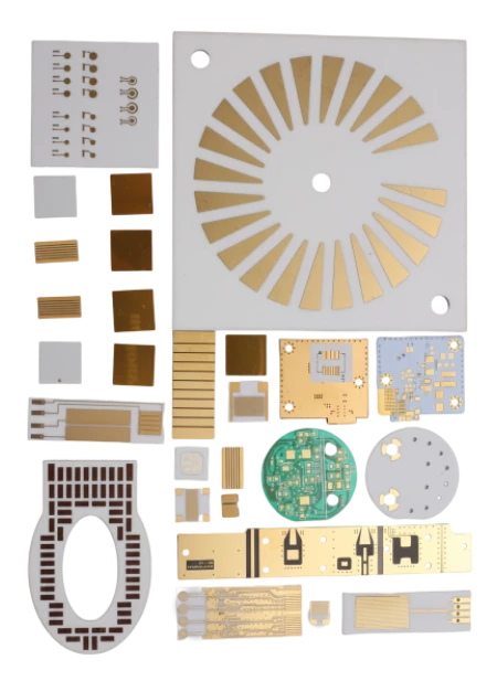
Reflow and thermal profile for ceramic refers to the specific temperature-versus-time curve applied during the soldering process of components onto ceramic substrates. Unlike standard organic substrates (like FR4), ceramic PCBs—typically made from Alumina ($Al_2O_3$) or Aluminum Nitride ($AlN$)—possess unique physical properties that dictate how they absorb and release heat.
At APTPCB (APTPCB PCB Factory), we define this process not just as melting solder, but as managing thermal stress. The scope includes the preheat phase, flux activation (soak), reflow (liquidus), and cooling. The boundaries of this process are strict: if the temperature rises too fast, the ceramic cracks; if it rises too slow, the flux exhausts before wetting occurs.
This profiling is distinct from standard PCB assembly because ceramics act as efficient heat sinks. They pull heat away from the solder joint rapidly. Therefore, the thermal profile must account for the energy required to heat the heavy thermal mass of the ceramic while protecting sensitive components. It is the intersection of material science and thermodynamics.
For more on the base materials involved, you can explore our capabilities in Ceramic PCB manufacturing.
reflow and thermal profile for ceramic metrics that matter (how to evaluate quality)
Once the definition is clear, we must quantify success using specific, measurable data points.
The quality of a ceramic reflow process is not subjective; it relies on precise thermal metrics. The table below outlines the critical parameters that engineers must monitor to ensure a reliable solder joint without damaging the brittle substrate.
| Metric | Why it matters | Typical Range / Factors | How to Measure |
|---|---|---|---|
| Ramp-Up Rate | Determines thermal shock risk. Ceramics fracture if heated unevenly or too quickly. | 0.5°C to 1.5°C per second. Never exceed 2°C/s for ceramics. | Thermal profiler slope calculation (Preheat zone). |
| Soak Time | Allows the ceramic mass to reach thermal equilibrium and activates flux. | 60 to 120 seconds. Longer than FR4 due to heat sink effect. | Time duration between 150°C and 190°C (for SAC305). |
| Time Above Liquidus (TAL) | Ensures intermetallic compound (IMC) formation for joint strength. | 45 to 90 seconds. Too short = cold joints; Too long = grain growth. | Time duration solder remains molten (e.g., >217°C). |
| Peak Temperature | The maximum temperature reached. Must melt solder but spare components. | 235°C to 245°C. Usually 15-25°C above liquidus. | Thermocouple reading at the component body and joint. |
| Cooling Rate | Critical for grain structure and preventing thermal shock fractures. | < 3°C to 4°C per second. Slower than FR4 to reduce stress. | Slope calculation from Peak to Solidus. |
| Delta T ($\Delta T$) | The temperature difference across the board. | < 10°C. Ceramics dissipate heat well, but large boards need care. | Difference between hottest and coldest thermocouple. |
How to choose reflow and thermal profile for ceramic: selection guidance by scenario (trade-offs)
With the metrics established, we must apply them to real-world manufacturing situations where trade-offs are inevitable.
Different ceramic applications require adjusted strategies. A "one-size-fits-all" profile does not exist for APTPCB clients. Below are common scenarios and the necessary adjustments.
1. High-Power LED Assembly (Aluminum Nitride)
- Scenario: Mounting high-wattage LEDs on AlN for maximum heat dissipation.
- Trade-off: AlN conducts heat very fast.
- Guidance: Increase the soak time significantly. The substrate will pull heat away from the pads. You need more thermal energy to ensure the solder paste reaches wetting temperature simultaneously with the component leads.
2. RF/Microwave Circuits (Alumina)
- Scenario: High-frequency circuits with sensitive gold plating.
- Trade-off: Gold embrittlement risk and component sensitivity.
- Guidance: Keep Peak Temperature on the lower end of the allowable range. Use a profile that minimizes TAL to prevent excessive leaching of gold into the solder joint.
3. Hybrid Assembly (Ceramic + Heavy Copper)
- Scenario: Ceramic spacers or boards integrated with heavy copper features.
- Trade-off: Massive thermal mismatch.
- Guidance: Use a "Saddle" profile (long soak). The heavy copper needs time to heat up. If you ramp too fast, the ceramic heats up, but the copper remains cold, leading to cold solder joints.
4. Fine-Pitch BGA on Ceramic
- Scenario: Densely packed Ball Grid Arrays on a ceramic interposer.
- Trade-off: Voiding potential and warping (though ceramic warps less than FR4).
- Guidance: Focus on the flux outgassing during the soak phase. A gradual ramp allows volatiles to escape before the solder melts, reducing voiding in the BGA balls.
5. Double-Sided Ceramic Assembly
- Scenario: Components on both top and bottom.
- Trade-off: Reflowing the first side again; thermal stress accumulation.
- Guidance: Use a lower peak temperature for the second pass if possible, or use a high-melting-point solder for the first side. Ensure the cooling rate is strictly controlled to prevent stress compounding.
6. Low-Temperature Solder (BiSn) Application
- Scenario: Using Bismuth-Tin solder to protect heat-sensitive sensors.
- Trade-off: Brittle joints vs. thermal safety.
- Guidance: The profile peaks much lower (around 170°C). However, the ramp rate must still be slow. Even if the peak is low, a fast jump from room temp to 170°C can still crack a large ceramic wafer.
For general assembly capabilities that support these scenarios, refer to our SMT and THT assembly services.
reflow and thermal profile for ceramic implementation checkpoints (design to manufacturing)

Selecting the right scenario is theoretical; executing it requires a disciplined step-by-step process.
To successfully implement a reflow and thermal profile for ceramic, follow these checkpoints. Each step includes a recommendation, a risk if ignored, and an acceptance method.
1. Pad Design & Thermal Relief
- Recommendation: Avoid direct connections to large metal planes without thermal relief.
- Risk: Tombstoning or cold joints due to heat sinking.
- Acceptance: DFM Review of Gerber files.
2. Solder Paste Selection
- Recommendation: Use a paste with a flux specifically designed for high-temp or long-soak profiles.
- Risk: Flux burnout before reflow (graping).
- Acceptance: Wetting test on a sample coupon.
3. Stencil Thickness Control
- Recommendation: Precision laser-cut stencils, typically 4-5 mils thick for fine pitch.
- Risk: Excess solder causes bridging; too little causes opens.
- Acceptance: SPI (Solder Paste Inspection) volume data.
4. Thermocouple Attachment
- Recommendation: Attach thermocouples using high-temp solder or conductive epoxy, not Kapton tape alone.
- Risk: Inaccurate readings leading to a wrong profile.
- Acceptance: Physical pull test on thermocouple wires.
5. Oven Zone Setup
- Recommendation: Configure oven zones to allow a slow ramp (add zones if necessary).
- Risk: Exceeding the 2°C/s ramp limit.
- Acceptance: Profiler simulation software check.
6. First Article Profiling
- Recommendation: Run a "Golden Board" (sacrificial board) with sensors.
- Risk: Guessing the thermal mass effect.
- Acceptance: Profile graph overlay against spec limits.
7. Nitrogen Environment (Optional but Recommended)
- Recommendation: Use $N_2$ reflow to widen the process window.
- Risk: Oxidation on difficult-to-solder ceramic surfaces.
- Acceptance: Visual inspection for shiny, smooth joints.
8. Cooling Slope Verification
- Recommendation: Ensure active cooling fans are not set to 100% immediately.
- Risk: Ceramic substrate fracture.
- Acceptance: Slope measurement on the cool-down curve.
9. X-Ray Inspection
- Recommendation: Mandatory for BGAs and large pads on ceramic.
- Risk: Hidden voids or cracks in the solder.
- Acceptance: X-Ray Inspection pass rate > 99%.
10. Visual Inspection for Micro-Cracks
- Recommendation: Inspect the ceramic edges and corners under magnification.
- Risk: Latent failure in the field.
- Acceptance: AOI (Automated Optical Inspection) at high magnification.
reflow and thermal profile for ceramic common mistakes (and the correct approach)
Even with a checklist, specific errors plague ceramic assembly; identifying them prevents costly scrap.
1. Treating Ceramic like FR4
- Mistake: Using a standard "universal" profile with a 3°C/s ramp.
- Correction: Always limit the ramp to < 2°C/s. Ceramics do not have the elasticity of epoxy-glass.
2. Ignoring Thermal Mass Differences
- Mistake: Profiling a bare board and assuming it matches a populated board.
- Correction: Profile a fully populated board. The components and the ceramic substrate together define the thermal mass.
3. Inadequate Soak Time
- Mistake: Rushing through the soak zone to speed up production.
- Correction: Extend the soak. Ceramics take longer to reach equilibrium. A short soak leads to "cold" solder in the center of large pads.
4. Rapid Cooling
- Mistake: Blasting the board with cold air to handle it sooner.
- Correction: Controlled cooling is vital. The CTE mismatch between the solder, component, and ceramic is highest during cooling.
5. Poor Thermocouple Placement
- Mistake: Placing sensors only on the PCB surface, not the component leads.
- Correction: Place sensors on the ceramic surface, the component body, and the solder joint to see the Delta T.
6. Overlooking Moisture
- Mistake: Reflowing ceramics that have absorbed moisture without baking.
- Correction: While ceramics absorb less than FR4, trapped moisture can still cause delamination or "popcorning" in sensitive layers. Bake if necessary.
reflow and thermal profile for ceramic FAQ (cost, lead time, Design for Manufacturability (DFM) files, stackup, Automated Optical Inspection (AOI) inspection, X-ray inspection)
Q: What is the maximum ramp rate for ceramic PCBs? A: We recommend keeping it below 2°C per second. Ideally, aim for 1°C to 1.5°C per second to minimize thermal shock risk.
Q: Why is the soak zone more critical for ceramics? A: Ceramics are excellent heat conductors. They pull heat away from the solder paste rapidly. A longer soak ensures the entire assembly reaches the flux activation temperature uniformly before the reflow spike.
Q: Can I use standard SAC305 solder for ceramic assembly? A: Yes, SAC305 is commonly used. However, the profile must be adjusted for its higher melting point (217°C) compared to leaded solder, ensuring the ceramic isn't shocked by the high peak temp.
Q: How does LED MCPCB assembly and reflow differ? A: LED MCPCBs (often using dielectric on metal or ceramic) require strict void management. Voids impede heat transfer, killing the LED. The profile must focus on outgassing flux completely before the solder solidifies.
Q: Do ceramic PCBs require a nitrogen reflow oven? A: It is not strictly mandatory but highly recommended. Nitrogen reduces oxidation, improves wetting on the ceramic metallization, and allows for a slightly wider process window.
Q: What causes "tombstoning" on ceramic boards? A: Uneven heating. If one pad heats faster than the other (common on ceramics if traces vary in width), the solder melts on one side first and pulls the component upright.
Q: How do I validate the profile without breaking the board? A: Use a "Golden Board" or a sacrificial sample that is fully populated. Attach thermocouples permanently to this board and run it through the oven to capture the data.
Q: Why do ceramics crack during cooling? A: Ceramics are brittle. If the solder contracts rapidly while the ceramic remains expanded (or vice versa due to CTE mismatch), the stress exceeds the ceramic's tensile strength.
reflow and thermal profile for ceramic glossary (key terms)
| Term | Definition |
|---|---|
| Alumina ($Al_2O_3$) | The most common ceramic substrate material, offering good thermal conductivity and electrical insulation. |
| Aluminum Nitride ($AlN$) | A high-performance ceramic substrate with extremely high thermal conductivity, used for high-power applications. |
| CTE (Coefficient of Thermal Expansion) | The rate at which a material expands when heated. Mismatch between ceramic and solder causes stress. |
| Liquidus | The temperature at which the solder alloy becomes completely liquid (e.g., ~217°C for SAC305). |
| Solidus | The temperature at which the solder alloy is completely solid. |
| Flux | Chemical agent in solder paste that removes oxides and promotes wetting. |
| Wetting | The ability of molten solder to spread and bond to the metal surface of the pad and component. |
| Voiding | Air or gas pockets trapped inside the hardened solder joint, reducing thermal and electrical performance. |
| Tombstoning | A defect where a component stands up on one end due to uneven wetting forces. |
| Thermal Shock | Structural failure caused by rapid temperature changes creating internal stress. |
| Soak Zone | The phase in reflow where temperature is held steady to activate flux and equalize board temperature. |
| Delta T ($\Delta T$) | The difference in temperature between the hottest and coldest parts of the assembly during reflow. |
Conclusion (next steps)
Mastering the reflow and thermal profile for ceramic is about balancing thermal energy. It requires a shift in mindset from standard FR4 processing to a precision-controlled thermal management strategy. By respecting the ramp rates, extending soak times, and validating with real-world data, you can achieve high-reliability joints on even the most brittle substrates.
At APTPCB, we specialize in these advanced assembly techniques. If you are preparing a project involving ceramic substrates, early engagement is key.
For a DFM review or Quote, please provide:
- Gerber Files: Including paste, solder mask, and copper layers.
- Stackup Details: Specifying ceramic type (Alumina or AlN) and thickness.
- Component BOM: To identify high-mass components that affect profiling.
- Test Requirements: Specify if X-ray or specific shear testing is required.
Ensure your ceramic designs are manufactured with the precision they demand. Visit our Quote page to start your project today.