
Contents
- Highlights
- What Is Reliability Test Matrix PCB? (Scope & Boundaries)
- Metrics That Matter (How to Evaluate It)
- How to Choose (Material & Design Selection)
- Implementation Checkpoints (from Design to Fab)
- Common Mistakes (and How to Avoid Them)
- Supplier Qualification Checklist: How to Vet Your Fab
- Glossary
- 6 Essential Rules for Reliability Test Matrix PCB (Cheat Sheet)
- FAQ
- Request a Quote / DFM Review for Reliability Test Matrix PCB
- Conclusion
In the high-stakes world of electronics manufacturing, a printed circuit board (PCB) is only as good as its ability to survive its intended environment. Whether it is an automotive ECU subjected to constant vibration and thermal cycling, or an aerospace controller facing the vacuum of space, the difference between a successful product and a catastrophic field failure often lies in a single document: the reliability test matrix pcb.
At APTPCB, we often see engineers focus heavily on the functional test plan (does it work right now?) while overlooking the reliability matrix (will it work in 5 years?). A robust reliability matrix is not merely a checklist; it is a comprehensive validation strategy that correlates design intent, material properties, and manufacturing process controls against specific industry standards (such as IPC-6012 Class 3 or AEC-Q100).
This guide serves as your definitive engineering resource. We will move beyond basic definitions to explore how to construct a matrix that ensures yield, longevity, and compliance.
Highlights
- Scope Definition: Differentiating between Qualification (Prototype) and Conformance (Mass Production) testing.
- Critical Metrics: Understanding MTBF, CTE mismatch, and Weibull distribution in the context of PCB failure.
- Material Science: How substrate selection (Tg, Td, CTE) dictates your test parameters.
- Test Methods: Deep dives into Thermal Shock, HAST, IST, and CAF testing.
- Implementation: A 4-step roadmap from design simulation to physical lab validation.
- Vendor Vetting: Specific questions to ask your fabrication partner to ensure they can execute your matrix.
What Is Reliability Test Matrix PCB? (Scope & Boundaries)
A reliability test matrix pcb is a structured document that defines the specific battery of stress tests, sample sizes, durations, and acceptance criteria a PCB must undergo to validate its design and manufacturing quality. Unlike a functional test, which checks electrical logic, the reliability matrix stresses the physical and chemical integrity of the board.
It acts as the "contract" between the design engineering team and the manufacturing floor. A well-designed matrix addresses three distinct phases of the product lifecycle:
- Design Qualification: Proving that the materials and stack-up can survive the mission profile (e.g., 1000 cycles of thermal shock).
- Lot Acceptance (Conformance): Proving that this specific batch was manufactured correctly (e.g., solder float test, microsectioning).
- Ongoing Reliability Monitoring (ORM): Periodic testing of production samples to ensure process drift hasn't occurred over months of production.
The matrix must align with the "Mission Profile" of the device. A consumer toy (IPC Class 1) requires a vastly different matrix than a medical pacemaker (IPC Class 3).
Tech Feature → Buyer Impact
| Technical Feature / Decision | Direct Impact (Yield/Reliability) |
|---|---|
| Interconnect Stress Testing (IST) | Accelerates barrel crack detection by 10x compared to traditional ovens; prevents intermittent field failures in high-via-count boards. |
| Conductive Anodic Filament (CAF) Testing | Critical for high-voltage/high-density designs; prevents internal short circuits caused by electrochemical migration over time. |
| Solder Float (288°C / 10s) | Simulates assembly reflow stress; immediately identifies delamination risks or weak copper-to-resin bonding. |
| Highly Accelerated Stress Test (HAST) | Rapidly identifies moisture absorption issues in laminates, crucial for outdoor or humid environment electronics. |
Metrics That Matter (How to Evaluate It)
When constructing your reliability test matrix, you cannot simply ask for "good quality." You must define quantifiable metrics. The following parameters are the industry standard for evaluating PCB robustness.
| Metric | Definition | Standard (Reference) | Typical Target (Class 2/3) |
|---|---|---|---|
| Tg (Glass Transition Temp) | The temp where resin turns from rigid to soft. | IPC-TM-650 2.4.25 | >150°C (Mid) / >170°C (High) |
| CTE-z (Z-axis Expansion) | How much the board expands in thickness with heat. | IPC-TM-650 2.4.24 | < 3.0% (50°C to 260°C) |
| T260 / T288 | Time to delamination at 260°C or 288°C. | IPC-TM-650 2.4.24.1 | > 30 minutes (T260) |
| Moisture Absorption | Percentage of weight gain after humidity exposure. | IPC-TM-650 2.6.2.1 | < 0.20% |
| Dielectric Breakdown | Voltage at which the insulation fails. | IPC-TM-650 2.5.6 | > 40kV/mm |
| Peel Strength | Force required to peel copper foil from the base. | IPC-TM-650 2.4.8 | > 1.05 N/mm (after stress) |
Why these matter: If your CTE-z is too high, the resin expands faster than the copper barrel during reflow, ripping the copper plating apart (barrel crack). This is the #1 cause of open circuits in multilayer boards. By specifying a strict CTE metric in your matrix, you force the selection of robust materials.
How to Choose (Material & Design Selection)
The foundation of any reliability matrix is the raw material. You cannot test quality into a board; you must design it in.
1. Material Selection
For high-reliability applications, standard FR4 is often insufficient. You must select laminates based on thermal performance.
- High-Tg Materials: For automotive or industrial applications, we recommend High Tg PCB materials (Tg > 170°C). These materials maintain mechanical stability at higher operating temperatures.
- Low-Loss Materials: For RF/Microwave applications, materials like Rogers or Teflon are required. However, these materials can be difficult to process. Your matrix must include specific peel strength tests to ensure the copper doesn't lift during assembly. Learn more about our Rogers PCB capabilities.
2. Design for Reliability (Dfr)
Your matrix should influence your design choices:
- Via Structure: If your matrix requires 1000 cycles of thermal shock (-40°C to +125°C), avoid stacked microvias if possible, or ensure your aspect ratio is conservative (below 0.8:1 for microvias).
- Copper Balance: Unbalanced copper causes warpage during reflow. Your matrix should include a "Bow and Twist" test (IPC-TM-650 2.4.22) to validate the stack-up design.
Implementation Checkpoints (from Design to Fab)
Implementing a reliability test matrix is not a one-time event; it is a roadmap that runs parallel to your manufacturing process.
Implementation Roadmap
From Concept to Production
Before fabrication, define the "Mission Profile" (temp range, lifespan, vibration). Use DFM tools to simulate impedance and stack-up stress. Define the test coupons (IPC-2221) that will be printed on the panel rails.
Produce a "Golden Lot." Subject these boards to destructive testing: Thermal Shock (1000 cycles), HAST, and Cross-Sectioning. This validates that the design *can* be manufactured reliably.
Transition to non-destructive or coupon-based testing. Implement Electrical Testing (Flying Probe/Bed of Nails) on 100% of boards. Perform microsections on 1 coupon per panel to verify plating thickness.
If a failure occurs (in lab or field), perform Root Cause Analysis (RCA). Use SEM (Scanning Electron Microscopy) to inspect interfaces. Update the matrix to include tests that catch this specific failure mode in the future.
Common Mistakes (and How to Avoid Them)
Even experienced engineers make errors when defining their reliability test matrix pcb.
- Testing the Board, Not the Coupon: Destructive testing on finished PCBA is expensive. Smart engineers design specific test coupons (IPC-2221 Type A/B) on the panel waste rails. These coupons represent the vias and traces of the main board but are designed for easy cross-sectioning and stress testing.
- Ignoring the "Use Environment": We often see clients request military-grade testing (MIL-PRF-31032) for consumer electronics. This drives up cost unnecessarily. Conversely, using standard IT-grade tests for Automotive Electronics is a recipe for recall.
- Overlooking Surface Finish: The reliability of the solder joint is heavily dependent on the surface finish (ENIG, HASL, OSP). Your matrix must include solderability testing (wetting balance) to ensure the finish hasn't expired or oxidized.
- Neglecting Mechanical Stress: Thermal stress is important, but vibration and drop testing are critical for handheld devices. Ensure your matrix includes mechanical shock testing if the device is portable.

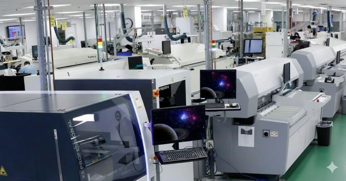
Supplier Qualification Checklist: How to Vet Your Fab
Before you trust a manufacturer with your reliability matrix, you must verify they have the capability to execute it. Use this checklist during your audit or RFQ process.
- In-House Lab: Does the factory have an in-house reliability lab (Thermal cycling chambers, X-ray, Cross-section equipment)? Outsourcing adds delay.
- IST Capability: Do they perform Interconnect Stress Testing (IST) or only traditional oven cycling? IST is faster and more accurate for via reliability.
- Plating Control: Do they use periodic pulse reverse plating (PPR) for high-aspect-ratio vias? Ask for their "Throwing Power" data.
- Cleanliness Testing: Do they perform Ionic Contamination testing (ROSE test) to prevent corrosion?
- Certifications: Are they certified to the standard you require (IATF 16949 for automotive, AS9100 for aerospace, ISO 13485 for medical)?
- Traceability: Can they trace a specific board back to the raw material lot and plating bath data?
For a deeper look at our quality systems, visit our Testing & Quality Assurance page.
Glossary
CAF (Conductive Anodic Filament): An electrochemical failure mode where a copper filament grows between two conductors inside the PCB laminate, causing a short circuit. IST (Interconnect Stress Testing): A method of testing PCB via reliability by rapidly cycling current through a specific coupon to induce thermal stress and measuring resistance changes. Tg (Glass Transition Temperature): The temperature at which the PCB substrate transitions from a hard, glassy state to a soft, rubbery state. Operating above Tg risks mechanical failure. Weibull Distribution: A statistical probability distribution used in reliability engineering to analyze life data and predict failure rates over time. Hipot Test: High Potential testing, used to verify electrical insulation by applying high voltage and checking for current leakage.
6 Essential Rules for Reliability Test Matrix PCB (Cheat Sheet)
| Golden Rule | Why It Matters | Implementation Key |
|---|---|---|
| 1. Define Mission Profile First | You can't test if you don't know the environment. | List Min/Max Temp, Vibration, and Lifespan (years). |
| 2. Use Representative Coupons | Testing the actual board is destructive and costly. | Design IPC-2221 coupons on panel rails. |
| 3. Prioritize Via Reliability | Vias are the weakest link in multilayer boards. | Mandate IST or Thermal Shock testing. |
| 4. Validate Material CTE | Z-axis expansion causes barrel cracks. | Choose materials with CTE < 3.5% (TMA). |
| 5. Don't Skip Solderability | A reliable board is useless if it can't be assembled. | Perform Wetting Balance tests on incoming lots. |
| 6. Close the Feedback Loop | Failures are learning opportunities. | Update the matrix after every RCA (Root Cause Analysis). |
FAQ
Q: How much does a full reliability qualification cost?
A: It varies significantly. A basic cross-section and solderability test might be included in standard NRE. However, a full 1000-cycle thermal shock or CAF testing campaign can cost thousands of dollars and take weeks. It is an investment in risk mitigation.
Q: What is the difference between ICT and Reliability Testing?
A: ICT (In-Circuit Test) checks for manufacturing defects (shorts, opens, wrong components) at the time of assembly. Reliability testing (like HAST or Thermal Cycling) stresses the board to predict future failures.
Q: Can I use standard FR4 for automotive applications?
A: Generally, no. Standard FR4 (Tg 130-140°C) cannot withstand the thermal cycling of an engine compartment. You typically need High-Tg (170°C+) materials.
Get Your Quote & DFM Review Now
Conclusion
A reliability test matrix pcb is not just paperwork; it is the engineering backbone of a successful product. By defining your metrics early, selecting the right materials, and partnering with a manufacturer like APTPCB that understands the physics of failure, you ensure your product lasts in the field. Contact APTPCB today to secure your reliability strategy.