Key Takeaways
- Definition: An RF connector launch assembly is not just the connector; it is the complete physical transition zone where energy moves from a coaxial cable mode to a planar PCB transmission line mode.
- Critical Metric: Voltage Standing Wave Ratio (VSWR) is the primary indicator of launch quality; a poor launch reflects energy back to the source.
- Design Reality: The PCB footprint (pad size, anti-pad clearance, and ground vias) often dictates performance more than the connector hardware itself.
- Manufacturing Tip: Solder volume control is vital; excess solder acts as a parasitic capacitor, degrading high-frequency signal integrity.
- Validation: Time Domain Reflectometry (TDR) is the standard method for isolating and measuring the impedance discontinuity at the launch point.
- Advanced Context: Processes like overmolding for RF front-end protection can detune a launch if the dielectric properties of the molding material are not accounted for.
- Partnership: Working with a specialized manufacturer like APTPCB (APTPCB PCB Factory) ensures that tight tolerance drilling and etching requirements are met.
What RF connector launch assembly really means (scope & boundaries)
The term RF connector launch assembly refers to the specific interface design and manufacturing process required to mount a radio frequency (RF) connector onto a printed circuit board (PCB). While a connector datasheet provides the specifications of the component itself, the "launch" is the system-level implementation. It encompasses the connector pin, the solder joint, the PCB landing pad, the ground reference planes, and the surrounding via structures.
In high-frequency electronics, the transition from a coaxial environment (the cable and connector) to a planar environment (microstrip, stripline, or coplanar waveguide on the PCB) creates a natural impedance discontinuity. If this transition is not optimized, the signal encounters a "bump" in the road. This causes reflections, signal loss, and potential data corruption.
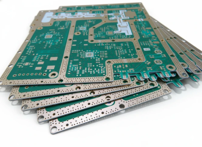
For engineers and procurement teams, understanding the launch assembly means looking beyond the part number. It involves analyzing how the PCB stackup interacts with the connector. At APTPCB, we see that successful launches depend heavily on the precision of the PCB fabrication—specifically the etching accuracy of the gap between the signal pad and the ground pour.
Metrics that matter (how to evaluate quality)
Evaluating an RF connector launch assembly requires specific quantitative metrics. These indicators tell you if the transition is electrically invisible or if it is acting as a bottleneck.
| Metric | Why it matters | Typical range or influencing factors | How to measure |
|---|---|---|---|
| VSWR (Voltage Standing Wave Ratio) | Indicates how much power is reflected due to impedance mismatch. A high VSWR means energy is bouncing back, potentially damaging sources. | < 1.3:1 is good for general RF. < 1.5:1 is acceptable for some commercial apps. < 1.1:1 is required for precision lab equipment. | Vector Network Analyzer (VNA). |
| Insertion Loss (IL) | Measures the signal power lost as it passes through the launch. High loss reduces range and signal quality. | Typically < 0.1 dB to 0.5 dB per launch, depending on frequency. Increases significantly above 10 GHz. | VNA (S21 parameter). |
| Return Loss | The inverse of VSWR, expressed in decibels. Higher absolute values indicate better matching. | > 20 dB is excellent. > 10 dB is often the minimum pass criteria for commercial devices. | VNA (S11 parameter). |
| Impedance Tolerance | The deviation from the target characteristic impedance (usually 50 Ohms). | ± 5% or ± 2 Ohms. Tighter tolerances require specialized PCB materials. | Time Domain Reflectometry (TDR). |
| Passive Intermodulation (PIM) | Critical in cellular systems. It measures unwanted signals generated by non-linearities (like bad solder joints). | < -150 dBc. Influenced by material purity and solder quality. | PIM Analyzer. |
| Bandwidth | The frequency range where the launch maintains acceptable VSWR. | Defined by the connector type (e.g., SMA up to 18 GHz, 2.92mm up to 40 GHz). | Frequency sweep testing. |
Selection guidance by scenario (trade-offs)
Choosing the right RF connector launch assembly strategy depends heavily on the operating environment and frequency. There is no "one size fits all" solution.
1. Sub-6 GHz Commercial (Wi-Fi, IoT, LoRa)
- Connector: SMA or RP-SMA (Edge Launch or Through-Hole).
- Trade-off: Through-hole offers mechanical strength but introduces parasitic inductance. Edge launch is better electrically but mechanically weaker.
- Recommendation: Use standard FR4 materials. Through-hole is acceptable if the stub is short.
2. High-Frequency 5G/Radar (24 GHz – 40 GHz)
- Connector: 2.92mm (K-type) or 2.4mm.
- Trade-off: Requires expensive high-frequency laminates (Rogers/Taconic). Solder wicking becomes a major variable.
- Recommendation: Use compression-mount connectors (solderless) to eliminate solder variability, or use precision surface mount with optimized footprints.
3. Automotive Radar & mmWave (77 GHz+)
- Connector: 1.85mm or 1.0mm, or waveguide transitions.
- Trade-off: Extremely sensitive to manufacturing tolerances. A 1-mil etching error can ruin performance.
- Recommendation: Requires High Frequency PCB fabrication with very tight tolerance control on copper features.
4. High-Vibration Aerospace/Defense
- Connector: SMP/SMPM (Blind mate) or Threaded TNC.
- Trade-off: Blind mate allows modular assembly but can suffer from "float" issues if not aligned perfectly.
- Recommendation: Use connectors with "limited detent" for retention. Ensure the PCB launch pad has redundant via stitching for mechanical strength.
5. High-Density Data Centers
- Connector: Multi-port SMPM or Ganged Coax.
- Trade-off: High density increases crosstalk risk between adjacent launches.
- Recommendation: Design robust ground isolation fences between channels.
6. Cost-Sensitive Consumer Electronics
- Connector: U.FL / IPEX (Micro-coax).
- Trade-off: Very low cycle life (only rated for ~30 matings). Not robust for external ports.
- Recommendation: Use for internal connections only. Ensure the cable is secured to prevent stress on the solder pads.
From design to manufacturing (implementation checkpoints)

Moving from a simulation to a physical RF connector launch assembly requires a disciplined process. Below is a checklist to guide the transition from engineering to the factory floor.
1. Stackup Definition
- Recommendation: Define the layer stackup early. The distance from the top layer to the first reference ground plane determines the width of the signal trace for 50 Ohms.
- Risk: Changing the stackup later changes the trace width, which mismatches the connector pin size.
- Acceptance: Verify stackup with an Impedance Calculator before layout.
2. Footprint Optimization (The "Anti-pad")
- Recommendation: The ground cutout (anti-pad) on inner layers below the launch pad must be sized to reduce capacitive coupling.
- Risk: If the anti-pad is too small, the launch will look capacitive (impedance dip). If too large, it looks inductive (impedance spike).
- Acceptance: 3D Electromagnetic simulation (HFSS/CST) is recommended for frequencies > 10 GHz.
3. Via Fencing (Stitching)
- Recommendation: Place ground vias around the launch pad to contain the electromagnetic field. Spacing should be less than 1/8th of the wavelength at the highest operating frequency.
- Risk: Sparse vias allow energy to leak into the PCB substrate, causing resonance and crosstalk.
- Acceptance: Visual inspection of Gerber files.
4. Solder Paste Stencil Design
- Recommendation: Use a step-stencil or reduced aperture opening for the center pin.
- Risk: Too much solder creates a "blob" that acts as a capacitor, ruining VSWR at high frequencies.
- Acceptance: Solder paste inspection (SPI) data.
5. Material Selection
- Recommendation: Match the connector pin width to the transmission line width. This often requires selecting a specific dielectric thickness.
- Risk: A wide trace going into a narrow connector pin creates a geometric step change that reflects signals.
- Acceptance: Review material datasheets for Dk (Dielectric Constant) stability.
6. Connector Placement Accuracy
- Recommendation: For edge launch connectors, the gap between the connector body and the PCB edge must be zero.
- Risk: An air gap creates an inductive discontinuity.
- Acceptance: Automated Optical Inspection (AOI) or X-Ray.
7. Reflow Profile Management
- Recommendation: RF connectors often have large metal bodies that act as heat sinks. The reflow profile must ensure the center pin reaches liquidus without overheating the dielectric.
- Risk: Cold solder joints on the ground lugs or melted internal dielectrics.
- Acceptance: Cross-section analysis during prototyping.
8. Post-Assembly Cleaning
- Recommendation: Remove all flux residues.
- Risk: Flux residues are hygroscopic and can alter the surface impedance over time, degrading performance.
- Acceptance: Ionic contamination testing.
9. Antenna Tuning and Trimming
- Recommendation: If the launch connects directly to an antenna, leave provision for matching components (pi-network).
- Risk: The theoretical antenna impedance rarely matches the real-world impedance perfectly.
- Acceptance: Antenna tuning and trimming on the first article to center the resonance frequency.
10. Final Validation
- Recommendation: Perform 100% or sample-based TDR testing.
- Risk: Shipping boards with hidden internal defects in the launch area.
- Acceptance: Testing & Quality reports showing pass/fail against impedance limits.
Common mistakes (and the correct approach)
Even experienced designers encounter issues with RF connector launch assembly. Here are the most frequent errors and how to fix them.
1. Ignoring the "Stub" in Through-Hole Launches
- Mistake: Using a standard through-hole SMA on a thick PCB where the signal is on the top layer. The unused portion of the pin (the stub) hanging below acts as an antenna.
- Correction: Use back-drilling to remove the stub, or use surface mount/edge launch connectors for high frequencies.
2. Overlooking Thermal Relief
- Mistake: Using standard thermal relief spokes on the ground pads of the connector.
- Correction: While thermal relief helps soldering, it adds inductance. For RF, direct connection to the ground plane is preferred. Pre-heat the board during assembly to compensate for the thermal mass.
3. Neglecting the Impact of Overmolding
- Mistake: Designing a perfect launch and then covering it with protective plastic without simulation.
- Correction: Overmolding for RF front-end modules changes the effective dielectric constant around the launch. This slows the wave velocity and lowers impedance. You must design the launch to be slightly inductive (higher impedance) to compensate for the capacitive effect of the overmold.
4. Poor Ground Return Path
- Mistake: Connecting the connector ground legs but failing to stitch the top ground to the inner reference planes immediately.
- Correction: Place ground vias as close as physically possible to the connector ground pads to minimize the return loop inductance.
5. Relying Solely on Datasheets
- Mistake: Assuming the connector performs exactly as the vendor's chart shows.
- Correction: Vendor charts usually show the connector on a reference test board. Your PCB material and stackup are different. Always simulate your specific launch geometry.
6. Incorrect Edge Plating
- Mistake: Not using edge plating (castellations) for edge-launch connectors.
- Correction: Edge plating ensures a continuous ground connection from the top to the bottom of the PCB, preventing radiation from the board edge.
FAQ
Q: What is the difference between an End Launch and a Vertical Launch? A: An End Launch connector mounts to the edge of the PCB, aligning the cable with the board plane. A Vertical Launch mounts on the surface, with the cable perpendicular to the board. Vertical launches are often used for test points or when board edge space is limited.
Q: Can I use a standard FR4 PCB for a 10 GHz launch? A: It is possible but difficult. FR4 has higher loss and less consistent dielectric properties than RF materials. For 10 GHz, the launch geometry must be extremely precise to compensate for the material's limitations.
Q: Why is TDR used for launch assembly validation? A: TDR (Time Domain Reflectometry) allows engineers to "see" inside the trace. It shows exactly where the impedance changes—whether it's at the solder joint, the pad, or the trace. This spatial resolution is critical for debugging.
Q: What is a "compression mount" connector? A: These connectors use screws to press the center pin against the PCB pad rather than soldering. They are reusable and eliminate solder variability, making them ideal for high-speed digital and mmWave applications.
Q: How does APTPCB handle high-frequency launch manufacturing? A: APTPCB utilizes advanced etching equipment to maintain trace width tolerances within +/- 10%. We also offer back-drilling and controlled depth drilling to optimize via stubs for RF performance.
Q: Does the connector plating matter? A: Yes. Gold plating is standard for RF because it resists oxidation and has excellent conductivity. However, the underplating (often Nickel) must be non-magnetic for PIM-sensitive applications.
Q: What is the "reference plane"? A: The reference plane is the continuous copper layer (usually Ground) immediately below the signal layer. The RF energy travels in the electromagnetic field between the trace and this plane.
Q: How do I specify launch requirements in my quote? A: Include the target frequency, the specific connector part number, the required impedance (e.g., 50 Ohms +/- 5%), and any TDR testing requirements.
Glossary (key terms)
| Term | Definition |
|---|---|
| Characteristic Impedance | The ratio of voltage to current for a wave traveling in one direction. Standard is 50 Ohms for RF. |
| VSWR | Voltage Standing Wave Ratio. A measure of how efficiently RF power is transmitted. |
| Return Loss | The loss of power in the signal returned/reflected by a discontinuity in a transmission line. |
| Insertion Loss | The loss of signal power resulting from the insertion of a device (connector) in a transmission line. |
| TDR | Time Domain Reflectometry. A measurement technique used to determine the impedance characteristics of transmission lines. |
| Microstrip | A type of transmission line consisting of a conductor on top of a dielectric with a single ground plane underneath. |
| Stripline | A conductor sandwiched between two ground planes within a dielectric. |
| CPW (Coplanar Waveguide) | A transmission line where the signal conductor and ground planes are on the same layer, separated by a gap. |
| Anti-pad | An area on a metal plane (power or ground) where copper is removed to allow a via or pin to pass through without shorting. |
| Skin Effect | The tendency of high-frequency alternating current to distribute itself near the surface of the conductor. |
| Cutoff Frequency | The frequency above which a specific mode of propagation can no longer be supported or where higher-order modes begin. |
| Back-drilling | The process of drilling out the unused portion of a plated through-hole (via stub) to reduce signal reflection. |
| PIM | Passive Intermodulation. Distortion caused by non-linearities in passive components like connectors. |
Conclusion (next steps)
The RF connector launch assembly is the gateway to your device's performance. A poorly designed launch can render an expensive RF chipset useless, while a well-optimized launch ensures signal integrity and system reliability. Success requires a holistic approach that combines precise stackup design, rigorous simulation, and flawless manufacturing execution.
Whether you are dealing with antenna tuning and trimming for an IoT device or complex overmolding for RF front-end modules in automotive radar, the physical details of the PCB matter.
Ready to build your high-frequency designs? To ensure your RF launch meets strict impedance and loss requirements, provide the following when requesting a quote:
- Gerber files with clear drill charts.
- Layer stackup details (material type and thickness).
- Target frequency and impedance specifications.
- Connector datasheets.
- Specific testing requirements (TDR, VNA).
Contact APTPCB today to review your design for manufacturing and ensure a successful launch.