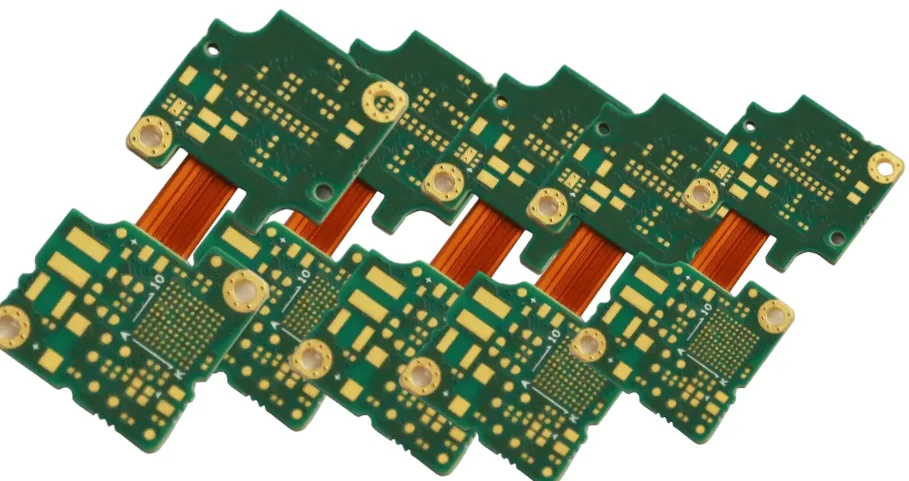
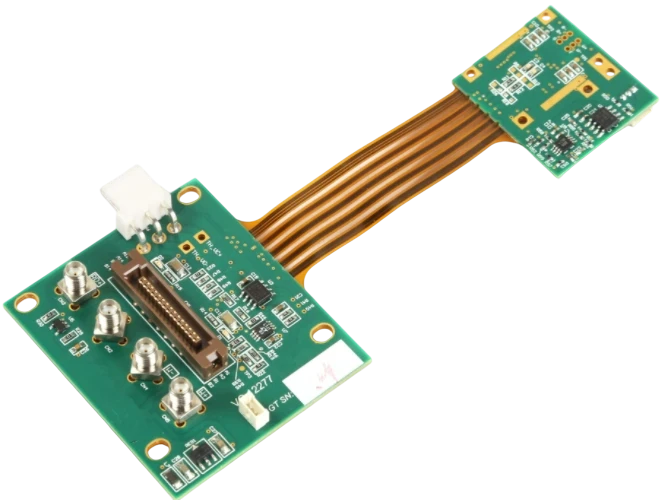
Rigid-flex printed circuit boards integrate the mechanical flexibility of polyimide with the structural integrity and high-density capabilities of rigid FR4 substrates. This hybrid architecture eliminates bulky connectors and wire harnesses, significantly reducing weight and improving reliability in aerospace, medical, and automotive applications. However, the successful deployment of rigid-flex technology requires strict adherence to complex design rules regarding stackup symmetry, material compatibility, and mechanical stress management.
Highlights
- Space Optimization: Reduces package volume by up to 60% compared to traditional wire harness assemblies.
- Reliability: Eliminates potential failure points at solder joints and crimps found in standard cabling.
- Signal Integrity: Provides controlled impedance and reduced parasitic inductance for high-speed signal transmission.
- 3D Packaging: Allows the PCB to fold and fit into irregular housing shapes during installation.
Rigid-Flex Specs at a Glance
| Parameter | Standard Specification | Advanced Capability | Critical Note |
|---|---|---|---|
| Flex Layers | 1–4 layers | 6–12+ layers | Keep flex layers in the center of the stackup (neutral axis). |
| Min Bend Radius (Static) | 10× Flex Thickness | 6× Flex Thickness | "Install-to-fit" applications only. |
| Min Bend Radius (Dynamic) | 20× Flex Thickness | 25×–40× Flex Thickness | For applications with continuous motion. |
| Trace Width/Space (Flex) | 4 mil / 4 mil (0.1mm) | 2 mil / 2 mil (0.05mm) | Wider traces preferred in bend zones to prevent cracking. |
| Drill-to-Copper (Flex) | 10 mil (0.25mm) | 6 mil (0.15mm) | Requires larger annular rings than rigid boards. |
| Impedance Control | ±10% | ±5% | Harder to control in flex regions due to dielectric variations. |
Contents
- Architecture and Stackup Configuration
- Material Selection Criteria
- Mechanical Design and Bend Radius
- Trace Routing and Signal Integrity
- Via Design and Plated Through Holes (Pth)
- Manufacturing Processes and DFM
- Surface Finishes and Reliability
- Assembly (PCBA) Challenges
- Cost Drivers and Optimization
- Quality Assurance and Testing
- Summary Checklist for Designers
Architecture and Stackup Configuration
The foundation of a robust rigid-flex PCB lies in its stackup. Unlike standard multilayer boards, rigid-flex stackups must account for Z-axis expansion mismatches between FR4 and polyimide, as well as the mechanical requirements of the flexible hinge.
The Neutral Axis Rule
The most critical mechanical design rule is placing the flexible circuit layers as close to the neutral axis of the stackup as possible. The neutral axis is the plane within the board where material experiences zero stress (neither compression nor tension) during bending.
- Rule: In a multilayer rigid-flex, the flex layers should be in the center.
- Why it matters: If flex layers are on the outer edges, they experience maximum tensile or compressive stress during bending, leading to copper work hardening and eventual fracture.
- Verification: Review the stackup diagram to ensure symmetry. If the rigid section has 8 layers, the flex layers should ideally be layers 4 and 5.
Unbalanced vs. Balanced Construction
While balanced construction is preferred to prevent warpage, certain designs require unbalanced stackups due to impedance or space constraints.
- Balanced Construction: Equal thickness of dielectrics and copper on both sides of the core. Minimizes bow and twist during reflow.
- Unbalanced Construction: Often necessary when specific layer counts are required for routing. Requires careful selection of "low-flow" prepregs to prevent excessive adhesive flow onto the flexible arm.
Air Gap Construction
For designs requiring extreme flexibility or a very tight bend radius, an "air gap" construction is used. Here, the flex layers are kept separate (unbonded) in the flexible region, allowing them to slide over each other like pages in a book.
- Range: Typically used when the flex section exceeds 4 layers.
- Benefit: Reduces the effective stiffness of the bundle.
- Trade-off: More complex manufacturing process and slightly reduced impedance control consistency.
Material Selection Criteria
Selecting the right materials is not just about electrical performance; it is about mechanical survival. The interaction between the rigid FR4, the flexible polyimide, and the adhesive systems determines the board's reliability.
Adhesive vs. Adhesiveless Polyimide
Polyimide (PI) cores come in two primary forms:
Adhesive-Based (Standard): Uses an acrylic or epoxy adhesive to bond copper to the PI.
- Pros: Lower cost, higher peel strength.
- Cons: The adhesive has a low Glass Transition Temperature (Tg) and high Z-axis thermal expansion. This is a common failure point in high-temperature assembly or operation.
- Limit: Avoid for high-reliability aerospace or automotive electronics PCB applications requiring extensive thermal cycling.
Adhesiveless (High Performance): Copper is cast or sputtered directly onto the PI.
- Pros: Thinner profile, better thermal stability, higher Tg.
- Cons: Higher material cost.
- Recommendation: Mandatory for HDI designs and rigid-flex boards with >4 layers.
Coverlay vs. Solder Mask
In the flexible section, standard liquid photo-imageable (LPI) solder mask is too brittle and will crack upon bending. Instead, a polyimide coverlay is used.
- Material: A layer of polyimide with an acrylic adhesive backing.
- Thickness: Typically 1 mil (25µm) PI + 1 mil (25µm) adhesive.
- Design Rule: Coverlay openings are drilled or laser-cut. Square openings are difficult; prefer circular or oval openings.
- Minimum Web: Maintain at least 10 mil (0.25mm) of coverlay web between pads to ensure adhesion.
For detailed material specifications, refer to our PCB materials guide.
Mechanical Design and Bend Radius
Calculating the minimum bend radius is essential to prevent copper fracturing. The allowable radius depends on whether the application is "static" (bend once to fit) or "dynamic" (continuous flexing).
Calculation Formulas
The minimum bend radius ($R$) is a function of the total thickness of the flex section ($h$).
1. Single-Sided Flex:
- Static: $R = 10 \times h$
- Dynamic: $R = 20 \times h$
2. Double-Sided Flex:
- Static: $R = 10 \times h$
- Dynamic: $R = 25 \times h$
3. Multilayer Flex:
- Static: $R = 20 \times h$
- Dynamic: Not recommended for high layer counts.
Common Failure: The I-Beam Effect
When traces on adjacent layers are stacked directly on top of each other, they increase the stiffness of the circuit in that localized area, creating an "I-Beam" effect.
- Rule: Stagger traces on adjacent layers in the bend zone.
- Why it matters: Stacking traces concentrates stress, leading to dielectric cracking and conductor fatigue.
- Verification: Check Gerber files for the flex region. Traces on Layer 2 should run in the spaces between traces on Layer 1.
Trace Routing and Signal Integrity
Routing signals across the rigid-to-flex transition requires specific techniques to maintain signal integrity and mechanical durability.
The Transition Zone
The interface where the rigid board meets the flexible tail is a high-stress area.
- Rule: Traces must cross the transition zone perpendicular (90°) to the rigid edge.
- Pitfall: Angled routing creates stress concentration points that can tear the copper during thermal expansion.
- Mitigation: Use "teardrops" on all pads and vias near the transition to add mechanical strength.
Impedance Control in Flex
Achieving controlled impedance in flex layers is more challenging than in rigid boards due to the lack of solid reference planes (often hatched to maintain flexibility).
- Reference Planes: Use cross-hatched copper (mesh) for ground planes in flex regions.
- Pattern: 45-degree hatch.
- Coverage: 50% to 70% copper density.
- Impact: Increases flexibility but increases trace impedance.
- Trace Width: Traces in flex regions often need to be wider than in rigid regions to match impedance targets (e.g., 50Ω) because the dielectric (polyimide + adhesive) is thinner than FR4.
- Verification: Use an impedance calculator specifically calibrated for hatched ground planes.
Necking Down
If high-density routing is required in the rigid section but flexibility is needed in the flex tail:
- Technique: Route with standard width in the rigid zone.
- Transition: "Neck down" (reduce width) smoothly as the trace enters the flex zone, but ensure the width remains sufficient for current carrying capacity.
- Limit: Avoid changing trace width exactly at the rigid-flex interface line. Perform the transition at least 30 mil (0.75mm) away from the edge.
Via Design and Plated Through Holes (Pth)
Vias are rigid structures. Placing them in flexible areas invites failure.
Placement Rules
- No Vias in Bend Areas: Never place a via in a section of the board intended to bend. The plating will crack.
- Keep-Out Zone: Maintain a minimum distance of 20 mil (0.5mm) from the rigid-to-flex interface for any vias.
- Pad Plating: Use "button plating" or selective plating pads to anchor the copper to the polyimide, preventing pad lifting during soldering.
Hdi and Microvias
For complex HDI PCB designs involving rigid-flex:
- Stacked Vias: Avoid stacking vias directly over the flex interface.
- Laser Drills: Laser drilling depth control is critical when stopping on a flex layer. The laser parameters for FR4 differ from those for polyimide.
- Aspect Ratio: Keep microvia aspect ratios below 0.8:1 to ensure reliable plating in the blind holes connecting rigid layers to the flex core.
Manufacturing Processes and DFM
Designing for Manufacturability (DFM) is distinct for rigid-flex due to the complex lamination cycles.
The "Bikini Cut" and Coverlay Placement
The coverlay does not extend across the entire rigid section. It usually penetrates the rigid section by a small amount to ensure a seal.
- Overlap: Coverlay should extend 15–30 mil (0.4–0.8mm) into the rigid section.
- Gap: Prepreg in the rigid section must not flow into the flexible area. Manufacturers use "no-flow" or "low-flow" prepreg.
- Adhesive Squeeze-Out: Allow for adhesive squeeze-out (flow) from the coverlay.
- Design Rule: Keep pads and features at least 10 mil (0.25mm) away from the coverlay edge to prevent adhesive from flowing onto solderable lands.
Strain Relief
Strain relief is mandatory at the rigid-flex interface.
- Epoxy Bead: A bead of flexible epoxy is often applied at the interface to stiffen the transition and prevent the flex circuit from bending at a sharp 90° angle against the rigid edge.
- Corner Fillets: Internal corners in the flex outline should have a minimum radius of 30 mil (0.75mm). Sharp 90° corners are stress risers that lead to tearing. Also, add a "tear-stop" copper feature (a dummy copper trace) along the edge of the flex circuit.
For a deeper dive into manufacturing constraints, consult our DFM guidelines.
Surface Finishes and Reliability
The surface finish affects both the shelf life and the mechanical durability of the assembly.
ENIG (Electroless Nickel Immersion Gold)
This is the standard finish for rigid-flex.
- Pros: Flat surface for fine-pitch components, excellent wire bonding capability.
- Flexibility: Nickel is brittle. While ENIG is fine for the rigid sections, excessive bending of ENIG-plated areas in the flex zone can cause micro-cracks.
- Rule: Do not apply surface finish to the dynamic bend area. Keep the copper bare (covered by coverlay) in the bend zone.
ENEPIG
For high-reliability wire bonding, ENEPIG (Electroless Nickel Electroless Palladium Immersion Gold) is preferred but more expensive.
Hot Air Solder Leveling (HASL)
- Avoid: HASL is generally not recommended for rigid-flex. The high thermal shock of the HASL process can delaminate the flex materials, and the uneven surface is poor for fine-pitch assembly.
Learn more about finish options in our surface finishes guide.
Assembly (PCBA) Challenges
Rigid-flex boards require specialized handling during PCBA assembly.
Moisture Management (Baking)
Polyimide is hygroscopic; it absorbs moisture from the air rapidly (up to 3% by weight).
- Risk: If moisture is trapped inside the polyimide during reflow soldering (240°C+), it turns to steam and causes delamination (popcorning).
- Procedure: Rigid-flex boards MUST be baked before assembly.
- Typical Cycle: 120°C for 2–4 hours immediately prior to soldering.
Fixturing
Flexible tails make the board floppy and difficult to handle in pick-and-place machines.
- Solution: Use custom pallets or fixtures to hold the flex flat during printing and placement.
- Design Tip: Include tooling holes in the waste area of the panel or in the rigid sections to aid in securing the board to the fixture.
Cost Drivers and Optimization
Rigid-flex PCBs are inherently more expensive than rigid boards—often 3x to 5x the cost. Optimizing the design can control these costs.
- Layer Count: Minimize the number of flex layers. A 2-layer flex core is significantly cheaper than a 4-layer flex core.
- Nesting: The shape of the flex tail impacts panel utilization. Curved or L-shaped tails waste material.
- Optimization: Design tails to be straight or foldable to allow tighter nesting on the production panel.
- Stiffeners: If a section of the flex needs to be rigid only for component support (and not for electrical routing), use a stiffener (FR4 or Polyimide) adhered to the flex, rather than creating a full rigid-flex stackup in that area.
Quality Assurance and Testing
To ensure the board meets the rigorous demands of aerospace and defense or medical sectors, specific tests are required.
- Thermal Shock: Cycling between -55°C and +125°C to test the integrity of plated through-holes (barrel cracks).
- Peel Strength Test: Verifies the bond strength between the copper and polyimide.
- Flexural Endurance: A specialized test where the board is bent repeatedly to the design radius to verify the cycle life (e.g., 100,000 cycles).
- Impedance Testing: Time Domain Reflectometry (TDR) coupons are placed on the panel to verify trace impedance in both rigid and flex regions.
Summary Checklist for Designers
Before submitting your Gerber files, run through this final checklist:
- Stackup: Are flex layers in the neutral axis?
- Bend Radius: Is the radius >10x thickness (static) or >20x (dynamic)?
- Transitions: Are traces perpendicular to the rigid-flex interface?
- Vias: Are all vias at least 20 mil away from the transition zone?
- Coverlay: Is there sufficient overlap (15+ mil) into the rigid section?
- Pads: Do pads in the flex zone have tie-downs (spurs) or larger annular rings?
- Tear Stops: Are copper tear stops included at internal corners?
Rigid-flex technology offers unmatched versatility for modern electronics. By adhering to these strict design guidelines and collaborating early with your manufacturer, you can produce highly reliable, compact, and performant interconnect solutions.