APTPCB specializes in advanced rigid-flex PCB design and fabrication, helping engineers turn complex 3D electronic architectures into reliable, manufacturable products. Our team supports customers from early stack-up planning through to mass production, ensuring every rigid-flex design meets mechanical, electrical, and assembly requirements.
This guide provides a practical, engineering-driven overview of rigid-flex PCB design, key manufacturing considerations, and the critical capabilities APTPCB offers to ensure stable yields and consistent performance. Whether you’re building aerospace modules, medical devices, automotive controllers, or high-density consumer electronics, this playbook will help you avoid common pitfalls and develop more robust rigid-flex solutions.
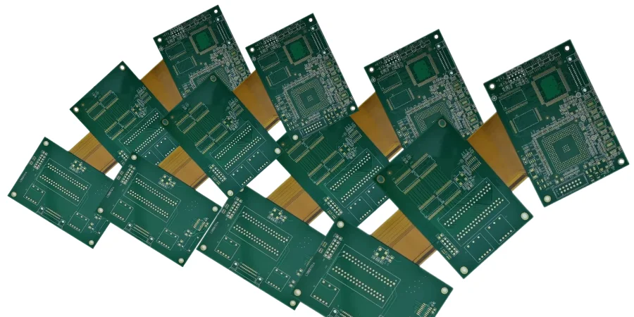
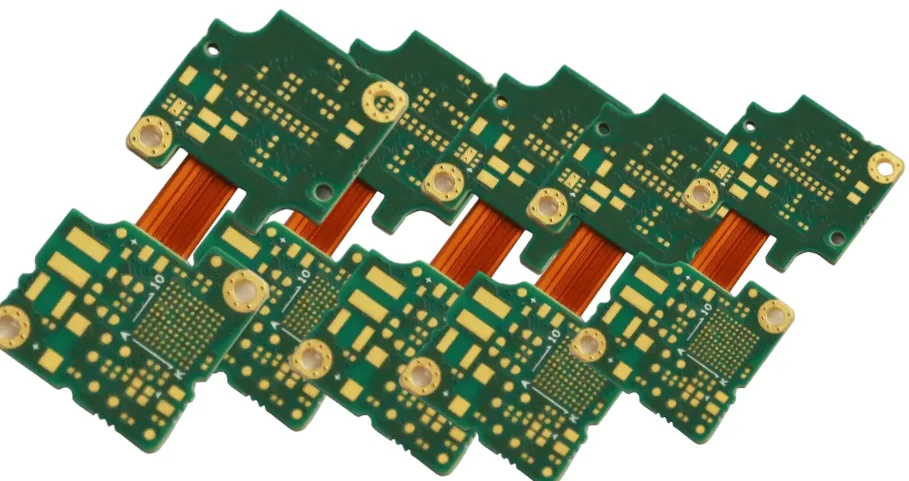
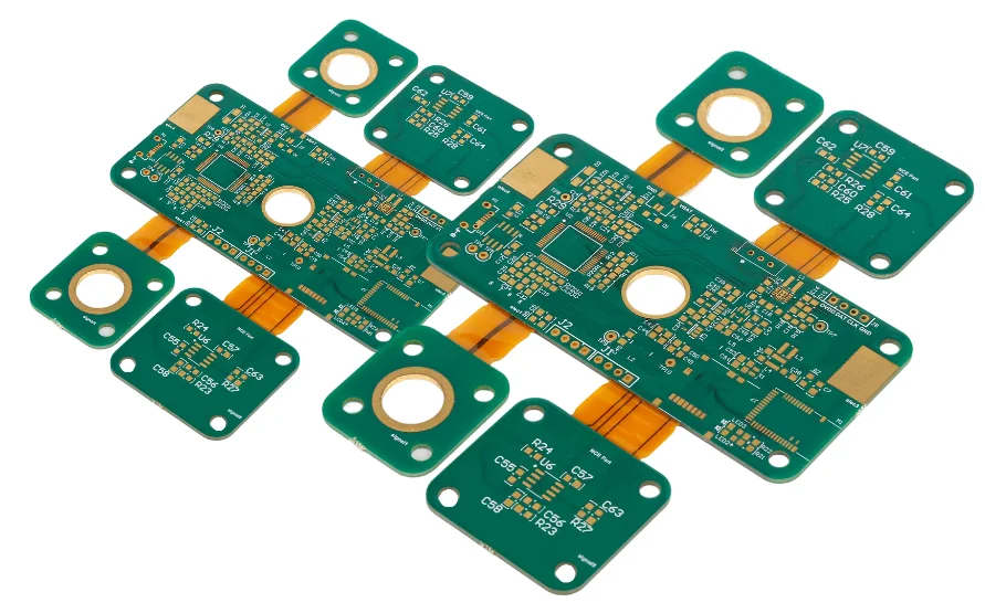
Understanding Rigid-Flex PCBs in Modern Electronics
Rigid-flex PCBs combine rigid FR-4 sections with flexible polyimide layers to create a single, continuous structure. The rigid areas support components and heat dissipation, while the flex sections enable 3D routing, bending, and direct interconnection without cables or separate connectors.
This hybrid approach reduces volume, simplifies wiring, and improves reliability in environments where vibration or movement is common. At APTPCB, we treat rigid-flex as a complete system-integration method—often replacing several rigid boards and harnesses with one optimized, highly reliable module.
Key Rigid-Flex Advantages and Application Scenarios
Space and Weight Optimization:
Rigid-flex boards allow circuits to fold around housings, hinges and curved surfaces, dramatically shrinking overall product size and mass.Reliability Improvement:
By eliminating discrete cables and connectors, rigid-flex architectures reduce the number of potential failure points, improving performance under shock, vibration, and long-term use.Greater Design Freedom:
Flex sections support dynamic bending and 3D interconnects, enabling more creative mechanical layouts and more ergonomic industrial designs.System-Level Cost Efficiency:
Although the bare rigid-flex PCB is more expensive per unit area than a simple rigid board, it can replace multiple boards, cables and assembly steps, often lowering total system cost in complex designs.Thermal and Mechanical Benefits:
Thin flex regions can provide more efficient heat spreading and relieve mechanical stress, while rigid zones maintain structural integrity and support heavy or heat-generating components.
Consistent Performance and Reliability
By understanding rigid-flex as an integrated electro-mechanical platform, APTPCB helps OEMs move beyond “just making it fit” toward designs that remain reliable over thousands of bend cycles and full product lifetimes. Every project starts with a clear view of where the product will bend, where loads and heat are concentrated, and how rigid and flex sections interact—so that reliability is engineered in from day one, not patched after failures appear.
Designing Robust Rigid-Flex PCBs: Core Engineering Principles
Rigid-flex PCB design is fundamentally more complex than designing rigid or flex boards in isolation. It requires balancing materials science, stack-up mechanics, electrical performance, and manufacturability within a single structure.
At APTPCB, we encourage designers to treat rigid-flex as a multidisciplinary engineering task: one where the right material, stack-up and geometry decisions are made early, before they become expensive to change.
Key Rigid-Flex Design Focus Areas
Material Selection as the Performance Foundation:
- Use polyimide (PI) films as the primary flex base for excellent high-temperature endurance, flexibility, and electrical stability (typical thickness: 12.5 μm, 25 μm, 50 μm).
- Choose rigid materials (standard FR-4, high-Tg FR-4, or high-speed/high-frequency laminates) according to signal speed, thermal demands, and reliability requirements.
- Decide between adhesiveless PI and adhesive-based constructions; adhesiveless PI laminated directly to copper offers better bend life and dimensional stability for dynamic flex.
- Apply coverlay (PI + adhesive) over flex traces instead of liquid solder mask to protect copper and preserve flexibility.
- Add stiffeners (FR-4, PI or metal) behind flex areas that carry connectors or components to distribute stress and provide local rigidity.
Stack-Up Design and Structural Symmetry:
- Design rigid and flex sections as one stack-up, ensuring smooth material and thickness transitions in rigid–flex interfaces to prevent stress concentration and delamination.
- Keep flex regions as symmetrical as possible in copper and dielectric layers to minimize warpage and uneven stress during bending.
- Use thinner copper weights (e.g., 0.5 oz or 1 oz) in flex sections to improve bendability; reserve thicker copper and heavier planes for rigid regions where current and thermal performance require it.
- In flex zones, consider grid or segmented copper patterns for ground and power to maintain flexibility while controlling EMI.
Bend Area Geometry and Routing Strategy:
- Respect minimum bend radius guidelines derived from total flex thickness and material data; tighter bends demand thinner and simpler stacks.
- Route conductors perpendicular to the bend axis in dynamic flex areas to minimize tensile and compressive strain along the length of copper traces.
- Maintain consistent trace width and spacing through bend regions; avoid sharp changes that create local stress points.
- Keep vias and plated through-holes out of dynamic bend areas; where vias are necessary, place them in static flex regions or use reinforced/filled structures with appropriate design rules.
Component Placement, Signal Integrity and Power Integrity:
- Place components primarily in rigid areas, especially heavy or heat-generating devices; avoid components in flex sections whenever possible.
- For high-speed and high-frequency signals, maintain controlled impedance, clean reference planes, and well-managed return paths as signals transition between rigid and flex layers.
- Ensure that power and ground conductors in flex zones maintain adequate current capacity and voltage drop performance while still permitting required bending.
Design for Manufacturability (DFM):
- Align minimum trace/space, via sizes, annular rings, and clearances with APTPCB’s rigid-flex process capabilities, especially in fine-pitch flex regions.
- Design rigid–flex transitions with sufficient adhesive overlap and rounded geometry (no sharp internal corners) to prevent cracking or peeling.
- Plan depanelization methods (routing, punching, laser cutting) in the outline and tooling features to avoid stress damage during final board separation.
Simulation and Early Co-Engineering:
- Use mechanical and electrical simulation tools (where available) to predict stress distribution, bending behavior and impedance before prototypes are built.
- Involve APTPCB’s engineering team early to validate stack-ups, materials, and bend regions, reducing the risk of late-stage design changes and yield loss.
Consistent Performance and Reliability
By focusing on material choice, stack-up symmetry, bend geometry, and manufacturability at the design stage, OEM engineers can dramatically increase the likelihood that the first rigid-flex prototypes already behave like production hardware. APTPCB’s DFM review closes the loop: we map design intent against real process windows, identify high-risk areas, and suggest targeted changes so that reliability and yield are built in before masks and tooling are ordered.
Manufacturing and Assembly Best Practices at APTPCB
Even a well-designed rigid-flex PCB can run into trouble if fabrication and assembly flows are not tuned to the specific behavior of flexible materials and complex laminations. Polyimide films, adhesives, and thin copper are more sensitive to moisture, temperature, and mechanical handling than standard FR-4.
APTPCB has established dedicated process controls for rigid-flex production that cover everything from material storage and lamination to drilling, surface finishing, SMT, and final packaging.
Key Manufacturing & Assembly Considerations
Material Storage and Handling:
- Store PI films, adhesives, and prepregs in controlled environments to manage humidity and temperature.
- Pre-bake materials where necessary to remove absorbed moisture and prevent voids, blisters, or delamination during lamination and reflow.
Lamination Process Control:
- Use precisely controlled temperature, pressure, and time profiles to laminate rigid and flex layers without damaging thin flex cores.
- Monitor resin flow and adhesive distribution carefully at rigid–flex interfaces to avoid voids, resin starvation, or excessive squeeze-out.
Drilling and Profiling for Flex Sections:
- Combine mechanical drilling for standard holes with laser drilling for microvias and sensitive flex zones to minimize mechanical stress.
- Apply high-precision registration systems to maintain alignment across multilayer flex and rigid-flex constructions.
- Use laser cutting or die punching for final profiling of flex outlines, reducing the risk of cracks, burrs, or local stretching.
Surface Finish and Uniformity:
- Tailor surface finishes (ENIG, ENEPIG, OSP, etc.) to the assembly process and application requirements, ensuring good solderability and corrosion resistance in both rigid and flex areas.
- Verify finish thickness and adhesion to prevent issues such as brittle interfaces or poor wire-bonding performance.
SMT Fixtures and Reflow Profiles:
- Design custom carriers and fixtures to support flex regions during SMT and reflow, preventing sagging, warping, or over-bending in the oven.
- Tune reflow profiles for the combined rigid-flex stack, avoiding excessive peak temperatures or dwell times that might damage adhesives or PI films.
- Prefer lighter, mechanically robust components in areas subject to flex-induced stress.
Testing, Inspection, Packaging and Transport:
- Apply AOI, flying-probe or fixture-based electrical testing to validate connectivity, especially in high-density regions and rigid–flex transitions.
- Perform mechanical tests (such as bend-cycle testing) where application requirements demand, particularly for dynamic-flex products.
- Use ESD-safe, moisture-controlled, and crush-resistant packaging that keeps flex regions supported and avoids unintended bending during shipping and handling.
Consistent Performance and Reliability
Through controlled material handling, precise lamination, and assembly processes designed specifically for rigid-flex, APTPCB delivers high-yield, stable production even for complex designs. Combining electrical testing with mechanical and visual inspection allows us to catch latent defects early, so the boards that reach your final assembly line already meet both performance and durability expectations.
Future Innovation Paths for Rigid-Flex PCB Technology
Rigid-flex PCB technology is evolving alongside the products that use it. As devices demand more functionality in smaller spaces, under harsher environmental and regulatory constraints, both materials and processes must continue to advance.
APTPCB monitors these developments and evaluates which emerging technologies are ready for real-world manufacturing, so customers can adopt innovation without compromising on reliability or cost.
Key Technology and Market Trends
Thinner, More Flexible Material Systems:
- Adoption of ultra-thin PI films and copper foils to support smaller bend radii and more aggressive folding structures.
- Wider availability of adhesiveless laminates for improved dynamic bend performance and dimensional stability.
Heterogeneous Integration and System-Level Packaging:
- Co-integration of rigid-flex PCBs with sensors, RF modules, optical components and antennas in compact, multi-function modules.
- Movement toward system-in-package (SiP) architectures where rigid-flex acts as both interconnect and mechanical backbone.
Advanced and Additive Manufacturing Methods:
- Exploration of 3D printing and additive copper deposition for fast-turn, complex rigid-flex geometries.
- Integration of embedded components and smart structures within rigid-flex stacks to reduce external packaging and wiring.
Sustainable and Eco-Friendly Materials:
- Development of halogen-free, recyclable materials that still meet high-performance and reliability targets.
- Process optimization to reduce waste, energy usage, and overall environmental footprint throughout the rigid-flex manufacturing cycle.
Enhanced Simulation and Digital Design Flows:
- Increasing use of multi-physics simulation to predict mechanical strain, thermal response, and signal integrity before the first prototype is built.
- Deeper integration of DFM rules and rigid-flex constraints directly into PCB CAD tools, accelerating design cycles and reducing iteration counts.
Consistent Performance and Reliability
APTPCB’s role in this evolving landscape is to filter and industrialize the most promising technologies. We validate new material systems and processes through controlled trials and standardized reliability testing, then introduce them into production only when they have proven stable. This approach allows customers to benefit from innovation—thinner boards, higher integration, more sustainable materials—without accepting uncontrolled risk.
Partnering with APTPCB for Next-Generation Rigid-Flex Projects
Rigid-flex PCB design is now a strategic capability for OEMs in aerospace, medical, automotive, industrial and high-end consumer sectors. Success depends on more than a good schematic or a clever mechanical layout; it requires a manufacturing partner who understands how design decisions show up as yield, reliability and cost on the factory floor.
APTPCB brings together rigid, flex and rigid-flex fabrication, plus assembly and test, under one technical and project-management framework. This allows your engineering and supply-chain teams to move from concept to mass production without constantly re-qualifying new suppliers or re-tuning processes.
Key Advantages of Working with APTPCB
Single Integrated Partner for Rigid, Flex and Rigid-Flex:
Simplify procurement, qualification, and communication by sourcing all PCB technologies—and PCBA—from one coordinated manufacturing platform.Early DFM/DFA Engagement:
Involve APTPCB’s engineering team at the concept and layout stages to validate materials, stack-ups, bend designs and assembly assumptions before committing to tooling.Scalable from Prototype to Volume:
Use the same core processes and quality systems for prototypes, pilot runs, and mass production, reducing surprises as volumes ramp.Industry Experience Across Key Applications:
Apply lessons learned from aerospace, medical, industrial and consumer projects to new designs, shortening learning curves and reducing technical risk.Continuous Improvement Over Product Lifetime:
Leverage real production and field data to refine designs, adjust materials or processes, and maintain consistent quality and cost competitiveness over the entire lifecycle.
Consistent Performance and Reliability
By partnering with APTPCB on rigid-flex PCB design and manufacturing, OEMs gain a long-term, engineering-focused ally who understands both the design challenges and the production realities of advanced electronics. Each project benefits from the experience of previous ones, building a foundation of proven stack-ups, materials, and process windows that support faster development, higher yields, and more reliable products.