As RF, microwave, and high-speed digital systems push into higher frequencies and tighter form factors, standard FR-4 boards increasingly hit their limits. Loss, dispersion, and poor impedance control quickly eat into link budgets and noise margins.
That’s why so many RF engineers, hardware architects, and system integrators are now searching for:
- “Rogers PCB manufacturing”
- “Rogers PCB fabrication for 5G and radar”
- “RF PCB manufacturer using Rogers high-frequency laminates”
Rogers high-frequency laminates have become a de-facto standard for low-loss, stable Dk/Df boards used in 5G infrastructure, radar, satellite communication, and high-speed backplanes. But designing and manufacturing with these materials is very different from standard FR-4.
As a PCB and PCBA factory experienced with Rogers and mixed-dielectric builds, we treat these projects as advanced RF engineering tasks, not just “another PCB job.” This article explains:
- Why Rogers materials are so important for RF and high-speed designs
- What makes Rogers PCB manufacturing technically challenging
- Key design practices for RF, microwave, and high-speed digital circuits on Rogers
- Typical application fields where Rogers PCBs really matter
- How to choose and work with a Rogers-capable PCB/PCBA partner
Why Rogers Materials Matter for High-Frequency & RF PCB Performance
When it comes to high-frequency PCB performance, material choice is just as important as layout. For many RF and microwave designs, the stack-up starts with Rogers laminates rather than FR-4 because of their controlled electrical behavior and low loss.
If your project involves controlled-impedance RF traces, antennas, couplers, filters, or high-speed serial links, it will typically sit in the same category as our dedicated high-frequency PCB manufacturing services.
Key Electrical Advantages of Rogers Laminates
Rogers offers several laminate families (RO4000, RO3000, RT/duroid, etc.), all optimized for RF and high-speed use. Across these families you’ll typically see:
Low Dielectric Loss (Low Df) Low loss tangent means less RF energy is absorbed by the dielectric as the signal travels. This is critical for:
- 5G base stations and small cells
- mmWave radar (24/77 GHz)
- Satellite and microwave links
- High-speed serial buses in servers and switches
Lower Df directly translates into longer reach, higher SNR, or more margin for filters and packaging loss.
Stable Dielectric Constant (Dk) vs. Frequency & Temperature Rogers materials are engineered for Dk consistency over a wide frequency and temperature range:
- Tighter impedance control over the operating band
- Better phase stability for antennas, filters, and phased-array systems
- Reduced drift over temperature cycling and environmental changes
Low Moisture Absorption Many RF systems live outdoors or in humid conditions. Low water uptake helps keep Dk, Df, and impedance stable over lifetime, rather than changing with weather.
Improved Thermal and Mechanical Stability Lower Z-axis CTE and balanced constructions improve:
- PTH reliability in multilayer RF backplanes
- Stability under solder reflow and repeated thermal cycling
- Mechanical robustness in harsh environments (automotive, aerospace, defense)
Together, these properties make Rogers the default choice for many customers who previously used generic FR-4 but hit the limits of signal integrity and repeatability. If you’re comparing options, our dedicated Rogers RF laminate overview is often a good starting point.
Consistent Performance and Reliability
By basing RF stack-ups on stable, low-loss Rogers materials, engineers gain predictable line impedance, insertion loss, and phase behavior. That predictability is what allows simulation, lab prototypes, and field performance to line up—even at tens of gigahertz and over wide temperature ranges.
For manufacturers, it also means that process windows, etch tolerances, and plating behavior can be tuned around a known dielectric system, enabling consistent impedance and loss across lots and over time.
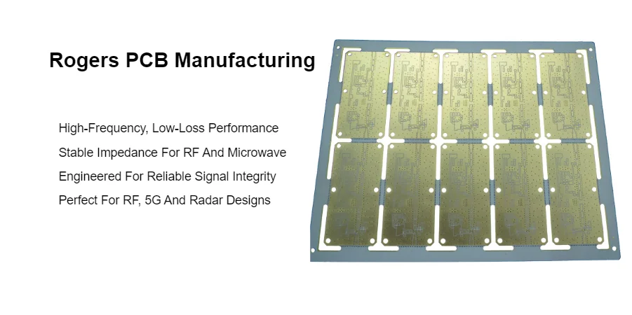
What Makes Rogers PCB Manufacturing Different from FR-4
Manufacturing a Rogers PCB is not just “running a different laminate through the same line.” PTFE-based and ceramic-filled materials behave very differently from FR-4 in drilling, surface prep, lamination, and plating.
If your application looks more like an RF front-end or microwave antenna than a standard digital board, it will fit naturally into our microwave PCB fabrication processes.
Key Process Challenges in Rogers PCB Fabrication
Drilling and Hole Quality PTFE and soft hydrocarbon laminates can:
- Smear into hole walls
- Generate burrs or “nailheading” at copper interfaces
- Be more sensitive to dull tools and wrong drill parameters
High-frequency boards demand clean, uniform holes for reliable plating and consistent via inductance. This requires:
- Optimized spindle speed and feed
- Special entry/backer materials
- Tight drill wear monitoring and replacement schedules
Desmear and Surface Activation Conventional FR-4 desmear recipes (permanganate, etc.) do not work on PTFE. For Rogers materials, you typically need:
- Plasma treatment tuned to the specific laminate
- Specialized chemistries for etchback and surface activation
- Careful control to avoid over-etching thin cores or under-treating high-Dk materials
Copper Adhesion and Surface Prep Some Rogers cores and bondplies have smooth, low-energy surfaces. To ensure robust copper adhesion:
- Micro-roughening, plasma, or chemical treatments must be tuned per material family
- Bondplies and copper foils must be selected together as a system
Fine-Line Etching and Impedance Control For RF microstrips, striplines, and couplers, etch tolerance directly impacts impedance and coupling. High-frequency Rogers boards often use:
- Thin cores and narrow traces
- Tight impedance tolerances (±5%, sometimes tighter)
That pushes etch uniformity, resist imaging, and plating control much harder than in commodity FR-4.
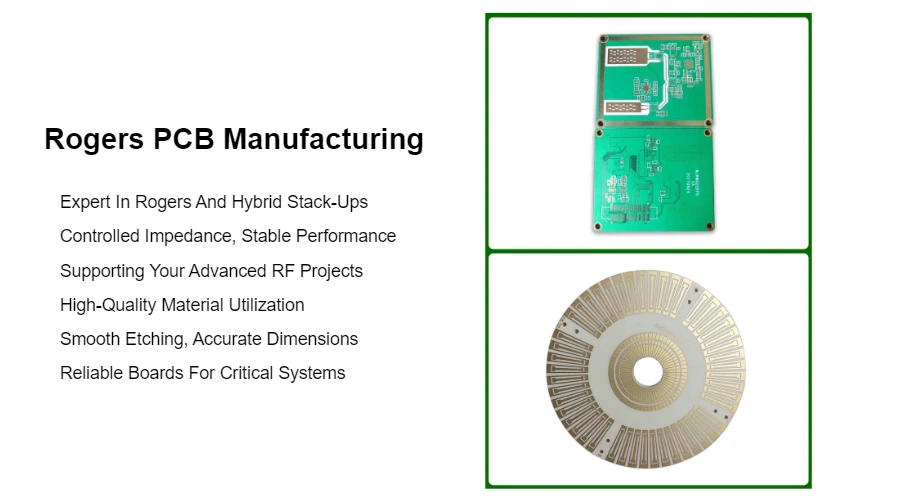
Hybrid Stack-Ups (Rogers + FR-4) Many designs combine:
- Rogers layers for RF sections
- FR-4 layers for digital, control, or power circuits
These “hybrid” structures require:
- Careful CTE matching
- Appropriate bondplies between dissimilar materials
- Lamination profiles that keep both resin systems in spec and avoid warp/twist
Material Cost and Yield Management Rogers laminates are significantly more expensive than standard FR-4. Scrapping a panel because of poor drill, smear, or lamination is much more painful. This is why Rogers projects are typically handled through our dedicated advanced PCB manufacturing workflows rather than generic production lines.
Consistent Performance and Reliability
A manufacturer that understands these process differences can produce Rogers PCBs with repeatable loss and impedance, high via reliability, and good panel flatness. One that doesn’t will struggle with random shifts in RF performance, intermittent via failures, and high scrap rates.
Designing Successful RF & High-Speed Circuits on Rogers PCBs
Rogers materials unlock better performance, but the design rules are not identical to FR-4. Successful RF and high-speed digital designs require stack-up, geometry, and layout choices that account for the properties of the laminate.
Material and Stack-Up Planning
Choose the Right Rogers Family Match material to:
- Operating frequency (e.g., RO4350B for sub-6 GHz, RO3003/RT/duroid for mmWave)
- Target Dk and loss tangent
- Power handling and thermal limits
- Budget and available thicknesses
Use Hybrid Stack-Ups Strategically Often you don’t need Rogers for every layer. Cost-optimized solutions use:
- Rogers for RF and critical high-speed layers
- FR-4 for control logic, power, and interfaces
Here, coordinating early on a PCB stack-up strategy will help you balance performance, cost, and manufacturability.
Define Impedance Targets and Tolerances Early For each interface (RF lines, differential pairs, backplane links), specify:
- Target impedance (e.g., 50 Ω single-ended, 100 Ω differential)
- Tolerance (±5%, ±7%, etc.)
- Frequency band of interest
This allows the fabricator to choose practical dielectric thicknesses and copper weights that hit your targets.
RF Layout & Transmission Line Design
Microstrip vs. Stripline Decide early whether RF traces run as:
- Microstrip (outer layer, one reference plane)
- Embedded microstrip (solder mask effects reduced)
- Stripline (inner layer between reference planes)
Each has different field distributions, parasitics, and Dk “seen” by the wave.
Trace Geometry and Modeling Use field-solver-based tools (not just closed-form equations) to set:
- Trace widths and gaps
- Reference plane spacing
- Edge-coupled vs. broadside-coupled structures
Then allow for etch compensation and plating growth in your geometry.
Via and Transition Design Vias are often the weakest link in RF paths:
- Keep via transitions out of the highest-frequency, most sensitive sections whenever possible
- Use multiple ground vias around RF transitions (via fences) to confine return currents
- Consider back-drilled vias or laser vias for very high-speed digital links
Grounding and Shielding Strategy
- Maintain continuous, well-stitched reference planes under RF traces
- Use stitching vias around filters, mixers, LNAs, and PAs
- Partition noisy digital/power areas from RF sections with intelligent floorplanning
Component Footprints, Thermal Design, and Assembly
RF-Optimized Pad and Land Patterns
- Avoid excessive pad size that increases capacitance
- Align component grounds properly with underlying ground planes
- Provide adequate pad-to-plane vias for low-inductance grounding
Thermal Considerations Power amplifiers, LNAs, and mixers on Rogers boards may dissipate significant heat:
- Use thermal vias under exposed pads
- Spread heat laterally with copper pours tied to ground
- Coordinate thermal design with the mechanical team (heat spreaders, chassis)
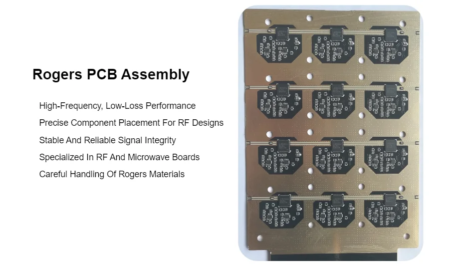
Assembly Constraints High-frequency boards often use fine-pitch BGAs, QFNs, and RF packages. Ensuring robust solder joints on Rogers substrates typically requires the same level of care as our BGA and fine-pitch assembly services.
Consistent Performance and Reliability
By treating stack-up and RF layout as an integrated design problem, rather than separate steps, you can dramatically reduce the gap between simulation and measured results. Combined with DFM input from the factory, many teams achieve close-to-final performance on the first or second spin, rather than after multiple trial-and-error cycles.
Where Rogers PCBs Are Used: Typical RF, Microwave & High-Speed Applications
Any project where loss, phase stability, or impedance accuracy is critical is a strong candidate for Rogers materials. In practice, we see Rogers PCBs used across a wide range of industries.
Typical Use Cases
Telecommunications & Wireless Infrastructure
- 5G NR sub-6 GHz and mmWave base stations
- Small cells, repeaters, and CPE equipment
- Point-to-point microwave links and backhaul radios
These fall squarely within our communication equipment PCB solutions.
Radar and Automotive Electronics
- 24 GHz and 77 GHz automotive radar units
- ADAS sensor modules and fusion ECUs
- Short-range industrial radar for presence and distance sensing
Aerospace, Defense & Avionics
- Airborne and ground-based radar arrays
- Satellite RF front-ends and payload electronics
- Secure communication and navigation systems
Server, Data Center & High-Speed Digital
- High-speed backplanes and line cards
- 25G/50G/100G+ SERDES channels
- Clock distribution and reference planes with strict jitter budgets
Test & Measurement, Medical, and Scientific
- RF instrumentation and network analyzers
- MRI coils and RF power stages
- Lab equipment for millimeter-wave and sub-THz research
In all these domains, Rogers PCB manufacturing is not just about hitting a geometry spec—it’s about delivering stable, repeatable RF behavior that can be modeled, built, and verified over and over again.
Choosing and Collaborating with a Rogers PCB Manufacturer
Once you know that your design requires Rogers materials, the next question is who should build it. Not every PCB shop that prints “Rogers capable” on a brochure has the depth in processes and engineering you need.
What to Look for in a Rogers-Capable Fabricator
Real Experience with Multiple Rogers Families
- Proven builds on RO4000, RO3000, RT/duroid, and similar laminates
- Ability to recommend a material for your band, power levels, and environment
Dedicated High-Frequency Processes
Optimized drilling and plasma for PTFE and hydrocarbon substrates
- Fine-line imaging and tight etch control for RF geometries
- Lamination profiles suited to hybrid Rogers/FR-4 stacks
Impedance and RF Performance Validation
- TDR or VNA-based impedance verification where required
- Clear documentation of stack-up, thicknesses, and tolerances
Engineering Support and DFM for RF
- Ability to review your layout, stack-up, and via strategy
- Practical suggestions for balancing RF performance, cost, and yield
Integrated PCB + PCBA Capability (Optional but Valuable)
- RF boards can be hard to assemble correctly; a shop that understands soldering, reflow, and inspection on Rogers substrates provides a shorter and safer path from Gerber to working hardware.
Typical Project Flow with a Rogers PCB Partner
A well-structured Rogers project usually follows these stages:
Early Concept & Material Discussion Align on target frequencies, interfaces, and likely material families.
Stack-Up Co-Design Define a manufacturable stack-up with realistic impedance and loss targets.
Layout with DFM/DFT Input Implement RF layouts informed by manufacturing capabilities.
Prototype Builds & Measurement Compare measured S-parameters and TDR data with simulation; fine-tune where needed.
Pilot and Volume Production Lock in process windows, testing strategy, and inspection criteria.
Lifecycle and Cost Optimization Adjust materials, panelization, or test coverage as volumes grow or requirements evolve.
Consistent Performance and Reliability
By treating your Rogers PCB fabricator as an engineering partner rather than just a supplier, you leverage their process knowledge and RF experience to de-risk your design. That collaboration is what turns a material spec into a stable, scalable high-frequency platform for your product line.
By combining the right Rogers laminate, a carefully engineered stack-up, RF-aware layout, and a manufacturing partner experienced in Rogers PCB manufacturing, you can confidently build RF, microwave, and high-speed digital hardware that meets demanding performance, reliability, and regulatory targets—project after project.