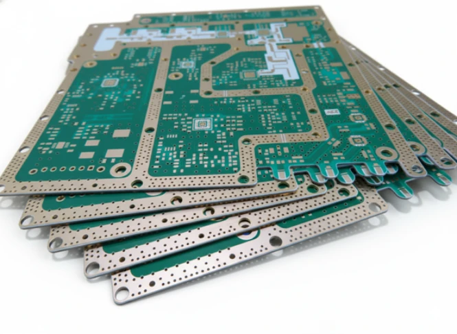
Satellite Terminal PCBs are the critical interface between ground-based user equipment and orbital networks. Whether connecting to a GEO Satellite PCB infrastructure for broadcast or a high-speed LEO Satellite PCB constellation for internet access, the terminal board must handle high-frequency signals (Ku, Ka, or V bands) with minimal loss while enduring harsh environmental conditions. APTPCB (APTPCB PCB Factory) specializes in fabricating these high-reliability boards, ensuring that complex phased array designs and mixed-signal stacks perform flawlessly in the field.
Satellite Terminal PCB quick answer (30 seconds)
Designing a Satellite Terminal PCB requires balancing high-frequency performance with thermal management and mechanical durability. Here are the critical takeaways for engineers:
- Material Selection is Critical: Standard FR4 is rarely sufficient for the RF front end. Hybrid stackups using PTFE-based laminates (like Rogers or Taconic) are standard to minimize dielectric loss.
- Controlled Impedance is Non-Negotiable: Signal integrity for Ku-band (12–18 GHz) and Ka-band (26.5–40 GHz) links demands strict impedance control, typically ±5% or tighter.
- Thermal Management for Amplifiers: Terminal Power Amplifiers (PAs) generate significant heat. Copper coin embedding or heavy copper layers are often required to dissipate heat from GaN components.
- HDI for Phased Arrays: Modern flat-panel terminals (like those for Starlink) utilize high-density interconnect (HDI) technology to route thousands of antenna elements within a compact footprint.
- Surface Finish Matters: ENIG or ENEPIG is preferred to ensure flat pads for fine-pitch components and wire bonding, preventing signal loss associated with HASL.
- Environmental Protection: Outdoor units (ODUs) face temperature cycling and humidity. The PCB must meet IPC-6012 Class 3 reliability standards to prevent barrel fatigue and delamination.
When Satellite Terminal PCB applies (and when it doesn’t)
Understanding when to deploy specialized Satellite Terminal PCB technology versus standard commercial boards is vital for cost and performance optimization.
When to use Satellite Terminal PCB technology:
- High-Frequency Communication: Systems operating in Ku, Ka, Q, or V bands where signal attenuation in standard materials is unacceptable.
- Phased Array Antennas: Electronically Steered Arrays (ESA) requiring complex multilayer stackups and precise phase matching between elements.
- Mobile Earth Stations: Terminals mounted on ships (maritime), aircraft (aero), or vehicles where vibration and thermal shock are constant.
- High-Power Transmission: Uplink terminals requiring robust thermal paths for Block Upconverters (BUCs) and Solid State Power Amplifiers (SSPAs).
- Mission-Critical Links: Defense or emergency response terminals where link failure is not an option.
When standard PCBs are sufficient (and Satellite Terminal specs are overkill):
- Low-Frequency Control Boards: Internal logic or power supply boards within the terminal enclosure that do not handle RF signals.
- GPS Receivers (Consumer Grade): Basic L1 GPS trackers often function adequately with standard FR4 materials.
- Prototype Logic Testing: Initial microcontroller firmware development boards that do not interface with the antenna.
- Low-Speed Telemetry: Systems using sub-1GHz frequencies (like LoRa) where standard FR4 dielectric loss is negligible.
Satellite Terminal PCB rules and specifications (key parameters and limits)
The following table outlines the essential design rules for a robust Satellite Terminal PCB. Adhering to these values ensures the board meets the stringent requirements of MEO Satellite PCB and LEO network providers.
| Rule | Recommended Value/Range | Why it matters | How to verify | If ignored |
|---|---|---|---|---|
| Dielectric Constant (Dk) | 3.0 – 3.5 (RF layers) | Determines signal speed and impedance; consistency is key for phase matching. | TDR (Time Domain Reflectometry) | Phase errors in antenna arrays; signal mismatch. |
| Dissipation Factor (Df) | < 0.0025 @ 10GHz | Minimizes signal attenuation (insertion loss) in high-frequency bands. | VNA (Vector Network Analyzer) | Excessive signal loss; reduced link budget/range. |
| Copper Roughness | VLP or HVLP (Very Low Profile) | Rough copper increases skin effect losses at high frequencies (>10GHz). | SEM (Scanning Electron Microscope) | Higher insertion loss than simulated; thermal rise. |
| Impedance Tolerance | ±5% (RF traces), ±10% (Digital) | Ensures maximum power transfer and minimizes reflections (VSWR). | Impedance Coupons / TDR | High VSWR; reflected power damages amplifiers. |
| Via Aspect Ratio | 8:1 to 10:1 (Through-hole) | Ensures reliable plating in deep holes; critical for ground continuity. | Cross-section analysis | Barrel cracks during thermal cycling; open circuits. |
| Layer-to-Layer Registration | ±3 mil (0.075mm) | Critical for coupling structures and broadside coupled lines. | X-Ray Inspection | Misaligned filters/couplers; detuned RF performance. |
| Thermal Via Pitch | 0.5mm – 1.0mm (under pads) | Efficiently transfers heat from PAs to the heatsink/ground plane. | Thermal Simulation / IR Cam | Component overheating; thermal shutdown or failure. |
| Surface Finish | ENIG or Immersion Silver | Provides flat surface for fine-pitch parts; avoids skin effect of nickel (if Silver). | Visual / XRF | Poor solder joints on BGAs; RF loss (if HASL used). |
| Peel Strength | > 0.8 N/mm (after thermal stress) | Prevents pads from lifting during rework or thermal cycling. | Peel Test | Pad lifting; reliability failure in field. |
| CTE (Z-axis) | < 50 ppm/°C | Prevents via barrel cracks during soldering and operation. | TMA (Thermomechanical Analysis) | Intermittent connections; early field failure. |
Satellite Terminal PCB implementation steps (process checkpoints)

Successfully manufacturing a Satellite Terminal PCB requires a disciplined workflow. APTPCB recommends the following steps to ensure the final product matches the design intent.
RF Link Budget & Material Selection
- Action: Select laminates based on operating frequency (e.g., Rogers RO4350B or Isola I-Tera MT40).
- Key Parameter: Df at target frequency (e.g., 30GHz for Ka-band).
- Check: Confirm material availability and lead time with the fabricator.
Stackup Design & Hybrid Configuration
- Action: Design a hybrid stackup using high-frequency materials for outer layers and FR4 for inner digital/power layers to save cost.
- Key Parameter: Core thickness and prepreg glass style (spread glass preferred).
- Check: Verify balanced construction to prevent warping.
Impedance & Phase Simulation
- Action: Simulate critical RF traces and antenna elements.
- Key Parameter: Line width and gap spacing.
- Check: Ensure simulated impedance is within fabricator capabilities (usually ±5%).
Thermal Management Layout
- Action: Place thermal vias under GaN/GaAs amplifiers and design coin inserts if necessary.
- Key Parameter: Via density and plating thickness (min 25µm).
- Check: Run thermal simulation to ensure junction temperatures stay below limits.
DFM Review (Design for Manufacturing)
- Action: Submit Gerbers for DFM to check minimum trace/space and aspect ratios.
- Key Parameter: Min trace width (e.g., 3 mil for HDI).
- Check: Resolve any "annular ring" violations or acid trap risks.
Fabrication (Etching & Lamination)
- Action: Precision etching and sequential lamination for HDI boards.
- Key Parameter: Etch factor and registration accuracy.
- Check: AOI (Automated Optical Inspection) of inner layers before lamination.
Surface Finish Application
- Action: Apply ENIG, ENEPIG, or Immersion Silver.
- Key Parameter: Gold/Nickel thickness consistency.
- Check: XRF measurement to verify thickness specs.
Electrical & RF Testing
- Action: Perform 100% netlist testing and TDR impedance verification.
- Key Parameter: TDR waveforms and continuity resistance.
- Check: Generate a test report confirming all impedance coupons passed.
Satellite Terminal PCB troubleshooting (failure modes and fixes)
Even with robust designs, issues can arise. Here is how to troubleshoot common Satellite Terminal PCB failures.
Symptom: High Insertion Loss (Low Gain)
- Causes: Wrong material Df, rough copper profile, or contamination on the surface.
- Checks: Verify material batch certs; check for solder mask residue on RF lines.
- Fix: Switch to VLP copper; remove solder mask from high-frequency traces.
- Prevention: Specify "solder mask defined" or "non-solder mask defined" clearly and use low-loss laminates.
Symptom: Intermittent Signal / Open Circuits
- Causes: Microvia fatigue, barrel cracks due to Z-axis expansion (CTE mismatch).
- Checks: Thermal shock testing; cross-section analysis of vias.
- Fix: Increase plating thickness; choose materials with lower Z-axis CTE.
- Prevention: Use stacked vias carefully; prefer staggered microvias for better reliability.
Symptom: PA Overheating / Thermal Shutdown
- Causes: Insufficient thermal vias, voiding in solder interface, or poor heatsink contact.
- Checks: X-ray inspection of BGA/QFN thermal pads (void percentage).
- Fix: Optimize reflow profile to reduce voids; increase thermal via count.
- Prevention: Implement metal-core or coin-embedded PCB technology for high-power sections.
Symptom: Passive Intermodulation (PIM)
- Causes: Ferromagnetic materials (Nickel) in the signal path, poor solder joints, or rusty connectors.
- Checks: PIM testing equipment; visual inspection of surface finish.
- Fix: Use Immersion Silver or OSP instead of ENIG for strictly PIM-sensitive lines (though ENIG is common, Nickel can be an issue at very high power).
- Prevention: Avoid sharp corners on traces; ensure clean, high-quality solder joints.
Symptom: Antenna Pattern Distortion
- Causes: Dielectric constant (Dk) variation across the board or layer misalignment.
- Checks: Measure Dk on coupons; check layer-to-layer registration.
- Fix: Use materials with tighter Dk tolerance; improve registration tooling.
- Prevention: Use "spread glass" weaves to minimize the fiber weave effect.
How to choose Satellite Terminal PCB (design decisions and trade-offs)
Selecting the right architecture for a Satellite Terminal PCB involves trading off cost, performance, and manufacturability.
1. Hybrid vs. Full High-Frequency Stackup
- Hybrid: Uses expensive RF materials (e.g., Rogers PCB materials) only on the top/bottom layers, with standard FR4 in the middle.
- Pros: Significantly lower cost; sufficient for most ground terminals.
- Cons: Complex lamination cycle; potential for warping due to CTE mismatch.
- Full RF Material: Entire board uses high-performance laminate.
- Pros: Best electrical consistency; simpler thermal expansion matching.
- Cons: Very high material cost; mechanically softer (harder to drill/route).
2. HDI vs. Through-Hole
- HDI (High Density Interconnect): Essential for HDI PCB designs like phased array antennas (Starlink/OneWeb) where pitch is extremely tight (< 0.65mm).
- Trade-off: Higher fabrication cost but enables compact, flat-panel designs.
- Through-Hole: Suitable for traditional parabolic dish feeds (BUC/LNB).
- Trade-off: Lower cost but limits component density and frequency performance due to via stubs.
3. Surface Finish Selection
- ENIG: Industry standard for flatness and reliability. Good for wire bonding.
- Immersion Silver: Better for very high frequency (skin effect) and lower cost, but tarnishes easily if not handled correctly.
- HASL: Generally avoided for Satellite Antenna PCB designs due to uneven surface and poor RF performance.
Satellite Terminal PCB FAQ (cost, lead time, common defects, acceptance criteria, Design for Manufacturability (DFM) files)
1. What is the typical lead time for a Satellite Terminal PCB? Standard lead time is 10–15 working days. However, if the design uses exotic materials (like specific Rogers or Taconic laminates) that are not in stock, lead time can extend to 3–4 weeks. Quick-turn options are available if materials are stocked.
2. How much does a Satellite Terminal PCB cost compared to a standard board? Due to specialized materials (RF laminates), tighter tolerances (impedance control), and often HDI structures, these boards typically cost 3x to 5x more than standard FR4 boards.
3. What are the acceptance criteria for these PCBs? Most satellite terminals require IPC-6012 Class 3 (High Reliability) performance. This mandates stricter plating thickness, annular ring requirements, and visual inspection standards compared to consumer electronics (Class 2).
4. Can you manufacture PCBs for LEO Satellite PCB user terminals? Yes. LEO terminals often use phased array antennas requiring complex HDI stackups, blind/buried vias, and precise Dk control. We have capabilities specifically suited for these high-density designs.
5. How do I prevent "Fiber Weave Effect" in my Satellite Terminal PCB? The fiber weave effect causes impedance variations when traces align with the glass weave. To prevent this, specify "spread glass" (e.g., 1067, 1078) or route traces at a slight angle (10°) relative to the weave.
6. What files are needed for a DFM review? We need Gerber files (RS-274X), a detailed stackup drawing (specifying material types and dielectric thicknesses), drill files (NC Drill), and IPC netlist. For RF boards, specifying the target frequency and impedance requirements is crucial.
7. Do you support metal-back or heavy copper for thermal management? Yes. For high-power terminals (uplink BUCs), we offer Metal Core PCB and heavy copper options to manage the heat generated by power amplifiers.
8. What is the difference between a Satellite Terminal PCB and a Satellite PCB? A Satellite PCB flies in space (on the satellite) and requires radiation hardening and outgassing control (NASA/ESA specs). A Satellite Terminal PCB stays on Earth (ground station/user terminal) and focuses on environmental durability (rain/humidity) and cost-efficiency for mass deployment.
9. How do you test controlled impedance on these boards? We place test coupons on the production panel that mimic the actual traces. We use TDR (Time Domain Reflectometry) to measure the impedance of these coupons to ensure they fall within the specified tolerance (e.g., 50Ω ±5%).
10. Is back-drilling necessary for Satellite Terminal PCBs? For high-speed digital lines or high-frequency RF passing through the board, via stubs can cause reflections. Back-drilling removes the unused portion of the via stub, improving signal integrity.
11. Can you handle mixed-dielectric (Hybrid) stackups? Yes, hybrid stackups are very common for satellite terminals to balance cost and performance. We are experienced in laminating dissimilar materials (e.g., FR4 + PTFE) without delamination or warping issues.
12. What is the maximum layer count for a phased array board? We can manufacture high-layer count boards (up to 40+ layers), but most commercial phased array terminals fall in the 8–16 layer range using HDI technology.
Resources for Satellite Terminal PCB (related pages and tools)
- Aerospace & Defense PCB Industry: Understand the broader context of high-reliability manufacturing standards.
- High Frequency PCB Capabilities: Detailed specs on RF materials and fabrication tolerances.
- Rogers PCB Materials: Specific data on the most common laminates used for satellite terminals.
- HDI PCB Technology: Essential reading for engineers designing compact phased array terminals.
- PCB Stackup Design: Guidelines on how to structure your hybrid board for success.
Satellite Terminal PCB glossary (key terms)
| Term | Definition |
|---|---|
| VSAT | Very Small Aperture Terminal; a two-way satellite ground station with a dish antenna. |
| Phased Array | An antenna array that creates a beam of radio waves which can be electronically steered without moving the antenna. |
| BUC | Block Upconverter; device used in the transmission (uplink) of satellite signals. |
| LNB | Low Noise Block downconverter; receiving device mounted on the satellite dish. |
| Ka-band | Microwave part of the electromagnetic spectrum (26.5–40 GHz), increasingly used for high-bandwidth satellite internet. |
| Ku-band | Microwave spectrum (12–18 GHz) primarily used for satellite TV and data VSATs. |
| Dk (Dielectric Constant) | A measure of a material's ability to store electrical energy; affects signal speed and impedance. |
| Df (Dissipation Factor) | A measure of the power loss rate of an electrical mode in a dissipative system; lower is better for RF. |
| CTE (Coefficient of Thermal Expansion) | How much a material expands when heated; mismatch causes reliability issues. |
| Hybrid Stackup | A PCB stackup that combines different materials (e.g., FR4 and Rogers) to optimize cost and performance. |
| TDR | Time Domain Reflectometry; a measurement technique used to determine the impedance of PCB traces. |
Request a quote for Satellite Terminal PCB (Design for Manufacturability (DFM) review + pricing)
Ready to move your Satellite Terminal PCB from design to production? APTPCB provides comprehensive DFM reviews to catch RF and mechanical issues before fabrication begins.
To get an accurate quote and DFM analysis, please provide:
- Gerber Files: RS-274X format preferred.
- Fabrication Drawing: Include material specs, stackup details, and impedance requirements.
- Quantity: Prototype (5–10 pcs) or Mass Production volume.
- Special Requirements: E.g., IPC Class 3, specific Rogers material, or back-drilling instructions.
Request Your Satellite Terminal PCB Quote Here – Our engineering team will review your files and respond within 24 hours.
Conclusion (next steps)
Designing a successful Satellite Terminal PCB requires a deep understanding of material science, RF engineering, and manufacturing constraints. Whether you are building a static VSAT unit or a dynamic mobile terminal for a LEO Satellite PCB constellation, the choice of fabricator is as critical as the design itself. By following the rules of impedance control, thermal management, and proper material selection outlined in this guide, you can ensure your terminal delivers reliable, high-speed connectivity in any environment.