Sourcing a Scene Control PCB requires balancing high-speed wireless connectivity with robust power management in a compact footprint. Buyers must navigate complex trade-offs between thermal performance, signal integrity, and manufacturing costs to ensure the final device reliably manages smart environments. This guide provides a structured approach to specifying, validating, and purchasing these critical control boards.
Highlights
- Scope Definition: Clarifies the difference between standard logic boards and integrated Scene Control PCBs.
- Risk Mitigation: Identifies root causes for common failures like RF interference and thermal throttling.
- Validation Protocols: Outlines essential tests for voice recognition accuracy and wireless range.
- Supplier Checklist: Provides a ready-to-use audit list for qualifying manufacturing partners.
Key Takeaways
Before diving into the technical details, here is a summary of the critical decision points for procurement teams.
| Decision Point | Critical Factor | Buyer Action |
|---|---|---|
| Material Selection | Signal loss vs. Cost | Use standard FR-4 PCB for logic; consider high-frequency laminates only if operating above 5GHz. |
| Layer Count | Size vs. EMI Shielding | Plan for 4–6 layers to allow dedicated ground planes for noise suppression in Voice Control PCBs. |
| Assembly (PCBA) | Component Sourcing | Verify the supplier's ability to source specific RF modules and MEMS microphones. |
| Testing | Reliability | Mandate Functional Circuit Testing (FCT) to verify wireless pairing and scene execution logic. |
Scene Control PCB: Scope, Decision Context, and Success Criteria
A Scene Control PCB acts as the central nervous system for smart automation. Unlike a simple on/off switch, this board processes multiple inputs—voice commands, sensor data, or app signals—and triggers a complex set of outputs, known as a "scene." For example, a "Movie Mode" scene might simultaneously dim lights, lower motorized blinds, and turn on AV equipment.
The Three Pillars of Functionality
- Wireless Connectivity: The board almost always functions as a Wireless Control PCB. It must support protocols like Wi-Fi, Zigbee, Z-Wave, or Bluetooth Low Energy (BLE). This requires precise impedance control and antenna design.
- User Interface (UI) Processing: Many modern units are also Voice Control PCBs. They integrate MEMS (Micro-Electro-Mechanical Systems) microphones and Digital Signal Processors (DSP) to interpret wake words and commands locally or via the cloud.
- Power Management: The board often switches mains voltage (110V/220V) to control loads. This necessitates strict isolation between the low-voltage logic/RF sections and the high-voltage power sections.
Success Criteria
For a buyer, success is defined by three metrics:
- Latency: The time between a user command (voice or touch) and the scene activation must be imperceptible (<200ms).
- Reliability: The device must maintain wireless connection in crowded RF environments.
- Safety: High-voltage isolation must meet regulatory standards (UL, CE, IEC) to prevent shock hazards and fire risks.
Specifications to Define Upfront (Before You Commit)
| Parameter | Recommended value / option | Why it matters | How to verify |
|---|---|---|---|
| Layer count | 4–8 (typical), higher as needed | Drives cost, yield, and routing margin | Stackup + DFM report |
| Min trace/space | 4/4 mil (typical) | Impacts yield and lead time | DRC + fab capability |
| Via strategy | Through vias vs VIPPO vs microvias | Affects assembly reliability | Microsection + IPC criteria |
| Surface finish | ENIG/OSP/HASL | Impacts solderability and flatness | COC + solderability tests |
| Solder mask | Matte green (default) | AOI readability and bridging risk | AOI trial + mask registration |
| Test | Flying probe / ICT / FCT | Coverage vs cost trade-off | Coverage report + fixture plan |
| Acceptance class | IPC Class 2 / 3 | Defines defect limits | Drawing notes + inspection report |
| Lead time | Standard vs expedited | Schedule risk | Quote + capacity confirmation |
Defining clear specifications prevents scope creep and engineering change orders (ECOs) later in the production cycle. Below are the critical parameters to lock in during the design phase.
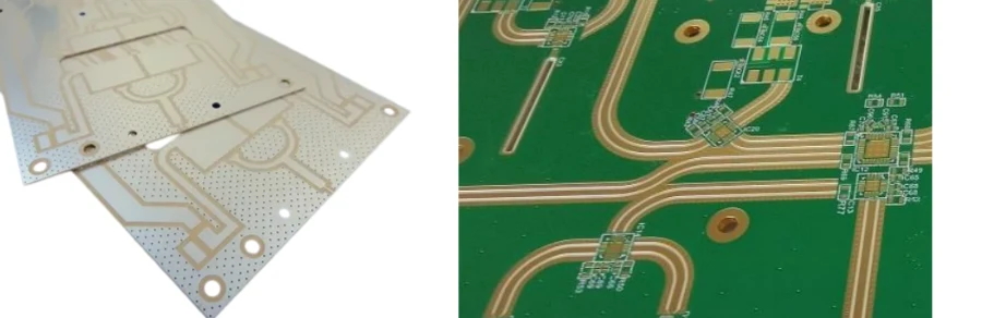
1. Stack-up and Layer Count
Scene Control PCBs typically require a 4-layer or 6-layer stack-up.
- Signal Layers: Top and bottom layers carry signals and components.
- Ground Planes: Internal layers are dedicated to ground. This is non-negotiable for a Voice Control PCB, as a solid ground plane shields sensitive microphone traces from digital noise.
- Power Planes: Dedicated power planes ensure stable current delivery to the RF module, preventing connection drops during transmission bursts.
2. Material Requirements
- Base Material: Standard FR-4 with a Tg (Glass Transition Temperature) of 150°C or higher is recommended. High Tg materials withstand the thermal stress of soldering RF modules and power relays.
- Dielectric Constant (Dk): For the Wireless Control PCB section, consistent Dk is vital. If using printed antennas, specify tight tolerance on the laminate thickness.
3. Copper Weight and Trace Width
- Logic Section: Standard 1oz (35µm) copper is sufficient.
- Power Section: If the board controls high-current loads (e.g., LED drivers or motors), use 2oz copper or wider traces.
- Trace Spacing: Adhere to creepage and clearance rules for high voltage. Typically, >6mm separation is required between primary (AC) and secondary (DC) sides.
4. Surface Finish
- ENIG (Electroless Nickel Immersion Gold): The preferred finish. It provides a flat surface for fine-pitch components like BGAs (Ball Grid Arrays) or QFNs (Quad Flat No-leads) used in microcontrollers and RF SoCs (System on Chip). It also offers excellent oxidation resistance.
5. Design for Manufacturability (DFM)
- Panelization: Define panel margins to fit assembly line conveyors.
- Fiducials: Ensure fiducial markers are present for automated optical inspection (AOI).
- Test Points: Mandate accessible test points for all critical nets (power rails, ground, data lines) to facilitate FCT Test fixtures.
Key Risks (Root Causes, Early Detection, Prevention)
Manufacturing Scene Control PCBs involves integrating noisy power electronics with sensitive RF and audio circuits. This combination creates specific risks that buyers must manage.
Risk 1: RF Desense (Receiver Desensitization)
- Root Cause: Digital noise from the microcontroller or switching noise from the power supply couples into the antenna.
- Impact: Reduced wireless range; the device shows "Offline" frequently.
- Prevention: Use shielding cans over the processor and memory. Ensure the antenna is placed away from high-speed digital lines. Request impedance control reports from the PCB fabricator.
Risk 2: Audio Interference in Voice Control
- Root Cause: Power supply ripple or ground loops introduce a "hum" into the microphone signal.
- Impact: Poor voice recognition; the device triggers falsely or fails to hear commands.
- Prevention: Use differential routing for microphone traces. Separate analog ground (AGND) and digital ground (DGND) and connect them at a single point (star ground).
Risk 3: Thermal Throttling
- Root Cause: Dimming circuits (Triacs or MOSFETs) generate significant heat. If the enclosure is small (e.g., in-wall switch), heat builds up.
- Impact: The processor slows down or shuts off to protect itself; plastic housing may warp.
- Prevention: Incorporate thermal vias to transfer heat to the ground plane. Use High Tg PCB materials. Simulate airflow during the design phase.
Risk 4: Component Availability
- Root Cause: Specific RF modules or specialized PMICs (Power Management ICs) may have long lead times.
- Impact: Production delays.
- Prevention: Validate the BOM (Bill of Materials) early. Identify drop-in replacements for passive components. Use a supplier with strong Component Sourcing networks.
Validation & Acceptance (Tests and Pass Criteria)
| Test / Check | Method | Pass criteria (example) | Evidence |
|---|---|---|---|
| Electrical continuity | Flying probe / fixture | 100% nets tested; no opens/shorts | E-test report |
| Critical dimensions | Measurement | Meets drawing tolerances | Inspection record |
| Plating / fill integrity | Microsection | No voids/cracks beyond IPC limits | Microsection photos |
| Solderability | Wetting test | Acceptable wetting; no de-wet | Solderability report |
| Warpage | Flatness measurement | Within spec (e.g., ≤0.75%) | Warpage record |
| Functional validation | FCT | All cases pass; log stored | FCT logs |
A robust validation plan ensures that the manufactured Scene Control PCB meets performance expectations. Do not rely solely on visual inspection.
1. Electrical Verification
- Flying Probe Test: For prototypes, checks for shorts and opens.
- In-Circuit Test (ICT): For mass production, verifies component values and placement.
2. Functional Performance Testing
- RF Performance: Measure Total Radiated Power (TRP) and Total Isotropic Sensitivity (TIS) in an anechoic chamber. Pass criteria: Wi-Fi signal strength > -70dBm at the edge of the defined range.
- Voice Quality: Run standardized audio files through the microphones and analyze the Signal-to-Noise Ratio (SNR). Pass criteria: SNR > 60dB.
- Load Testing: Connect the maximum rated load (e.g., 600W lighting) and run the "scene" continuously for 48 hours. Monitor temperature rise.
3. Environmental Stress Screening (Ess)
- Thermal Cycling: Cycle the board between -20°C and +85°C to check for solder joint fatigue, especially on rigid-flex interfaces if used.
- Humidity Test: Operate the board at 90% humidity to ensure conformal coating (if applied) prevents leakage currents.
Supplier Qualification Checklist (RFQ, Audit, Traceability)
When selecting a manufacturer for Scene Control PCBs, use this checklist to vet their capabilities.
General Capabilities
- ISO 9001 Certification: Verified and current.
- Smart Home Experience: Evidence of past projects involving IoT or home automation.
- Turnkey Service: Ability to handle PCB fabrication, component sourcing, and assembly under one roof.
Technical Competence
- Impedance Control: Can they provide TDR (Time Domain Reflectometry) reports for RF traces?
- HDI Capability: Do they support HDI PCB features like blind/buried vias if miniaturization is required?
- Conformal Coating: Do they have automated lines for applying protective coatings?
Quality Assurance
- AOI & X-Ray: Is Automated Optical Inspection used for all boards? Is X-Ray used for BGA/QFN inspection?
- Traceability: Can they trace every component on a specific board back to the supplier lot number?
- Firmware Flashing: Do they have the equipment to flash firmware and security keys onto the Wireless Control PCB during assembly?
How to Choose Scene Control PCB (Trade-Offs and Decision Rules)
Making the right choice involves balancing competing constraints. Here are common trade-offs and how to navigate them.
Trade-Off 1: Integrated Soc vs. Discrete Modules
- Option A (Module): Use a pre-certified RF module (e.g., ESP32 module).
- Pros: Faster time-to-market, simplified FCC/CE certification.
- Cons: Higher unit cost, larger footprint.
- Option B (Chip-down): Place the RF SoC and antenna directly on the PCB.
- Pros: Lower unit cost at high volume, flexible form factor.
- Cons: Complex RF design, expensive certification process.
- Decision Rule: If volume is <10k units/year, use a module. If >50k, go chip-down.
Trade-Off 2: Rigid vs. Rigid-Flex
- Option A (Rigid): Standard FR-4 board.
- Pros: Lowest cost, standard manufacturing.
- Cons: Limited by enclosure shape.
- Option B (Rigid-Flex): Combines rigid boards with flexible interconnects.
- Pros: Fits into complex 3D shapes (e.g., curved smart speakers), eliminates connectors.
- Cons: Higher cost, longer lead time.
- Decision Rule: Use Rigid-Flex PCB only if space constraints make connectors impossible or if vibration reliability is critical.
Trade-Off 3: On-Board vs. External Antenna
- Option A (PCB Antenna): Trace printed on the board.
- Pros: Free (no component cost).
- Cons: Larger board area, susceptible to interference from nearby metal.
- Option B (Ceramic/Chip Antenna): Surface mount component.
- Pros: Small, detuning resistant.
- Cons: Adds cost.
- Decision Rule: Use a PCB antenna for large devices (hubs). Use a chip antenna for small wearables or sensors.
FAQ (Cost, Lead Time, DFM Files, Materials, Testing)
Q: What drives the cost of a Scene Control PCB most significantly? The layer count and the inclusion of HDI (High Density Interconnect) features are primary drivers. Additionally, the cost of the RF module or SoC and specialized connectors can dominate the BOM.
Q: What files are required for a DFM review? You must provide Gerber files (RS-274X), the Drill file (Excellon), the BOM (Bill of Materials) with manufacturer part numbers, and the Pick-and-Place (Centroid) file. For Voice Control PCBs, specify the microphone port location clearly in the mechanical layer.
Q: How do I ensure my Voice Control PCB hears commands clearly? Mechanical design is as important as the PCB. Ensure the acoustic path (hole in the case) is sealed to the microphone on the PCB using a rubber gasket. On the PCB, surround the microphone with a ground ring.
Q: Can I use standard FR-4 for 5GHz Wi-Fi control boards? Yes, standard FR-4 is generally acceptable for Wi-Fi frequencies if the trace lengths are short. However, for longer RF traces, materials with lower loss tangents (like Isola or Rogers) may be necessary to maintain signal strength.
Q: What is the typical lead time for these boards? Standard prototype fabrication takes 3–5 days. Full turnkey assembly (including component sourcing) typically takes 2–4 weeks, depending on the availability of specific ICs.
Q: Do I need impedance control for a simple Zigbee switch? Yes. Even though Zigbee is low bandwidth, the 2.4GHz carrier frequency requires 50-ohm impedance matching between the radio and the antenna to prevent signal reflection and range loss.
Q: How are firmware updates handled during manufacturing? Suppliers can pre-program ICs before mounting or use a test jig with pogo pins to flash the firmware after assembly. This is often combined with the Functional Circuit Test (FCT).
Request a Quote / DFM Review for Scene Control PCB (What to Send)
To get an accurate quote and a thorough DFM Guidelines review, ensure your data package is complete. Missing information regarding impedance or stack-up is the most common cause of delays.
Checklist for Quote Request:
- Gerber Files: All layers, including solder mask and silkscreen.
- Fabrication Drawing: Specify material (Tg), thickness (e.g., 1.6mm), copper weight, and surface finish (ENIG recommended).
- Impedance Requirements: List specific nets and target impedance (e.g., "RF_OUT: 50 ohms").
- Assembly BOM: Include approved vendors for critical RF and power components.
- Test Requirements: Briefly describe if FCT or IC programming is needed.
Glossary (Key Terms)
| Term | Meaning | Why it matters in practice |
|---|---|---|
| DFM | Design for Manufacturability: layout rules that reduce defects. | Prevents rework, delays, and hidden cost. |
| AOI | Automated Optical Inspection used to find solder/assembly defects. | Improves coverage and catches early escapes. |
| ICT | In-Circuit Test that probes nets to verify opens/shorts/values. | Fast structural test for volume builds. |
| FCT | Functional Circuit Test that powers the board and checks behavior. | Validates real function under load. |
| Flying Probe | Fixtureless electrical test using moving probes on pads. | Good for prototypes and low/medium volume. |
| Netlist | Connectivity definition used to compare design vs manufactured PCB. | Catches opens/shorts before assembly. |
| Stackup | Layer build with cores/prepreg, copper weights, and thickness. | Drives impedance, warpage, and reliability. |
| Impedance | Controlled trace behavior for high-speed/RF signals (e.g., 50Ω). | Avoids reflections and signal integrity failures. |
| ENIG | Electroless Nickel Immersion Gold surface finish. | Balances solderability and flatness; watch nickel thickness. |
| OSP | Organic Solderability Preservative surface finish. | Low cost; sensitive to handling and multiple reflows. |
Conclusion (Next Steps)
Sourcing a Scene Control PCB is a multidisciplinary challenge that merges RF engineering, audio processing, and power electronics. By defining your stack-up and material requirements early, mitigating interference risks through proper grounding, and enforcing strict validation protocols, you can ensure your product delivers a seamless user experience.
The difference between a glitchy smart device and a market leader often lies in the quality of the PCB fabrication and assembly. Start by engaging with a manufacturer who understands the nuances of wireless and voice integration. Review your design against the DFM guidelines, validate your component supply chain, and prioritize rigorous testing to secure a successful product launch.