Definition, scope, and who this guide is for
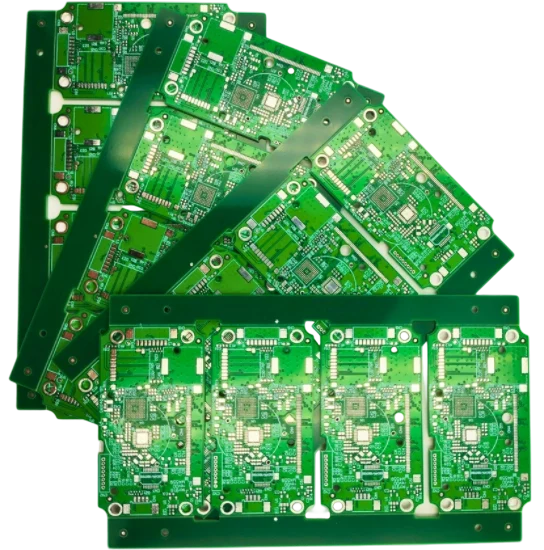
A Sequencing Batch PCB is the dedicated control hardware designed to manage sequential batch processes, most commonly found in wastewater treatment (Sequencing Batch Reactors or SBRs), industrial chemical dosing, and precision agriculture systems like aeroponics. Unlike general-purpose controller boards, these PCBs must execute precise timing logic—managing cycles of filling, reacting, settling, decanting, and idling—while surviving harsh, humid, and often corrosive environments. They act as the central nervous system, interfacing directly with high-current relays for pumps, analog sensors for pH/oxygen levels, and digital communication modules for remote monitoring.
For procurement leads and engineers, sourcing a Sequencing Batch PCB involves more than just matching a Gerber file to a manufacturer. It requires a deep understanding of environmental hardening, mixed-signal integrity (keeping sensitive sensor data away from noisy pump motors), and long-term reliability. A failure in this component does not just mean a stopped clock; it can lead to environmental non-compliance in wastewater plants or crop loss in aeroponic facilities.
This guide is written for decision-makers who need to move from a prototype or a PLC-based design to a scalable, custom PCB solution. It covers the specific material requirements, risk mitigation strategies, and validation protocols necessary to ensure your hardware performs flawlessly in the field. Whether you are building an Activated Sludge PCB controller or an Aeroponic Control PCB, the principles of durability and precise sequential logic remain the same.
At APTPCB (APTPCB PCB Factory), we have seen that the most successful projects start with clear specifications. This playbook provides the framework to define those specs, validate your supplier’s capabilities, and ensure that the final product meets the rigorous demands of industrial batch processing.
When to use Sequencing Batch PCB (and when a standard approach is better)
Deciding between a custom Sequencing Batch PCB and an off-the-shelf Programmable Logic Controller (PLC) is the first critical step in the sourcing process. While PLCs are excellent for one-off projects or extremely high-cost infrastructure where space is not an issue, a custom PCB becomes the superior choice as production volumes increase or when form factor and integration are critical.
Use a custom Sequencing Batch PCB when:
- Volume Justifies Cost: You are producing more than 100–500 units per year. The non-recurring engineering (NRE) costs of a custom board are quickly amortized, resulting in a significantly lower per-unit cost compared to buying industrial PLCs.
- Space is Constrained: You need to fit the controller, power supply, and relay drivers into a specific enclosure size that standard DIN-rail PLCs cannot accommodate.
- Integration is Required: You need to combine specific sensor interfaces (e.g., dissolved oxygen, pH, turbidity) directly onto the main board to reduce wiring harness complexity and improve signal integrity.
- IP Protection: You want to embed proprietary control algorithms or encryption that is harder to reverse-engineer than standard ladder logic on a PLC.
- Power Efficiency: Your application runs on solar or battery backup (common in remote aeroponic or small-scale sewage units), and you need low-power sleep modes that standard industrial controllers lack.
Stick to a Standard PLC or General Controller when:
- Prototyping: You are still refining the timing sequences (Fill, React, Settle) and need to change logic daily without re-spinning hardware.
- Ultra-Low Volume: You are building fewer than 50 units, and the high unit cost of a PLC is less than the development cost of a custom PCB.
- Extreme Flexibility: The end-user needs to reprogram the logic entirely in the field using standard industrial languages (Ladder, Function Block) without firmware engineering support.
Sequencing Batch PCB specifications (materials, stackup, tolerances)
Once you have determined that a custom Sequencing Batch PCB is the right path, the next step is defining the engineering specifications. These boards often sit at the intersection of power electronics (driving pumps) and sensitive instrumentation (reading sensors). The specifications must reflect this dual nature.
- Base Material (Laminate):
- Standard: FR-4 TG150 or TG170.
- Reason: Higher Glass Transition (Tg) temperatures are recommended not just for heat, but for better thermal cycling resistance in outdoor enclosures.
- Copper Weight:
- Power Layers: 2 oz to 3 oz (70µm to 105µm).
- Signal Layers: 1 oz (35µm).
- Reason: Heavy copper is essential for carrying current to solenoids, valves, and motors without excessive voltage drop or heating.
- Surface Finish:
- Preferred: ENIG (Electroless Nickel Immersion Gold).
- Reason: Provides excellent flatness for fine-pitch components and superior corrosion resistance compared to HASL, which is critical in humid treatment plant environments.
- Solder Mask:
- Type: High-quality LPI (Liquid Photoimageable).
- Color: Green or Blue (standard), but ensure the dam size is sufficient (min 4 mil) to prevent solder bridging on fine-pitch ICs.
- Conformal Coating:
- Requirement: Acrylic, Silicone, or Urethane coating is mandatory.
- Thickness: 25µm to 75µm.
- Reason: Protects against moisture, hydrogen sulfide (common in sewage), and fertilizer dust (aeroponics).
- Layer Stackup:
- Configuration: 4-Layer minimum recommended.
- Structure: Signal / Ground Plane / Power Plane / Signal.
- Reason: Dedicated ground and power planes provide shielding for sensitive analog sensor signals against the noise generated by relay switching.
- Trace Width & Spacing:
- High Voltage: Creepage and clearance must meet IPC-2221 standards for the operating voltage (e.g., >2.5mm for 220V mains if present on board).
- Signal: Standard 5 mil / 5 mil is usually sufficient.
- Via Protection:
- Spec: Tented or Plugged vias.
- Reason: Prevents flux entrapment and moisture ingress through the board, which can cause long-term corrosion.
- Component Selection:
- Grade: Industrial (-40°C to +85°C) rating for all active components.
- Connectors: Gold-plated contacts for sensor inputs; rugged terminal blocks for power outputs.
- Impedance Control:
- Requirement: Only if using high-speed communication (Ethernet, Wi-Fi modules).
- Tolerance: ±10% on differential pairs.
- Silkscreen & Marking:
- Detail: Clearly label all terminal blocks (e.g., "PUMP 1", "SENSOR pH") to aid field technicians during installation and maintenance.
- Documentation:
- Output: IPC-D-356 netlist for electrical test comparison, ODB++ or Gerber X2 for fabrication.
Sequencing Batch PCB manufacturing risks (root causes and prevention)
Manufacturing a Sequencing Batch PCB involves specific risks related to the environment it will inhabit and the load it controls. Understanding these risks allows you to preemptively address them in the design and procurement phase.
- Electrochemical Migration (ECM) / Dendrite Growth
- Root Cause: Moisture combining with ionic residues (flux) under a voltage bias creates conductive paths between traces.
- Detection: High-resistance shorts appearing after weeks of operation in humid environments.
- Prevention: Strict cleanliness requirements (ionic contamination testing) and high-quality conformal coating.
- Relay Contact Welding
- Root Cause: High inrush current from motors or pumps causes relay contacts to fuse shut.
- Detection: The "Fill" or "Decant" cycle never stops, leading to overflow.
- Prevention: Design in snubber circuits, varistors, or zero-crossing switching; specify high-inrush rated relays.
- Thermal Stress on Solder Joints
- Root Cause: Repeated heating (high load) and cooling cycles, or outdoor day/night temperature swings.
- Detection: Intermittent connections or cracked joints on heavy components like terminal blocks.
- Prevention: Use TG170 material; ensure thermal relief pads are designed correctly; consider underfill for large BGAs if used.
- Analog Signal Corruption
- Root Cause: Ground loops or electromagnetic interference (EMI) from switching inductive loads (pumps) affecting pH/DO sensor readings.
- Detection: Erratic sensor data during specific batch phases (e.g., when the aerator is on).
- Prevention: Separate analog and digital grounds; use 4-layer stackup with solid reference planes; keep high-voltage traces away from sensor inputs.
- Conformal Coating Delamination
- Root Cause: Poor surface preparation or incompatible flux residues preventing coating adhesion.
- Detection: Peeling or bubbling of the coating, visible under UV inspection.
- Prevention: Ensure the PCBA is thoroughly cleaned and dried before coating; verify flux/coating compatibility.
- Connector Oxidation
- Root Cause: Exposure to corrosive gases (H2S in wastewater) or high humidity.
- Detection: Intermittent signal loss or increased resistance in power connections.
- Prevention: Use gold plating on low-voltage contacts; use gas-tight terminal blocks; apply dielectric grease if necessary.
- Component Obsolescence
- Root Cause: Selecting niche components for critical timing or sensing functions that go EOL (End of Life).
- Detection: Supplier notifies of inability to source parts for the next batch.
- Prevention: Choose mainstream components; request a BOM health check during the quote phase.
- Firmware/Hardware Mismatch
- Root Cause: Updating PCB revision (e.g., pin swap) without updating the firmware bootloader.
- Detection: Board passes electrical test but fails functional logic test.
- Prevention: Implement strict revision control on the PCB silkscreen and within the firmware ID.
- Plated Through Hole (PTH) Fatigue
- Root Cause: Z-axis expansion of the PCB material during thermal cycling breaks the copper barrel in the via.
- Detection: Open circuits that appear only at high temperatures.
- Prevention: Use high-Tg materials; ensure proper copper plating thickness (min 20µm average).
- Inadequate Test Coverage
- Root Cause: Relying only on Flying Probe Test (FPT) which checks connectivity but not load handling.
- Detection: Boards fail when driving actual pumps in the field.
- Prevention: Implement Functional Circuit Testing (FCT) that simulates load currents.
Sequencing Batch PCB validation and acceptance (tests and pass criteria)

To ensure your Sequencing Batch PCB is ready for deployment, you must move beyond standard electrical testing. The validation plan should simulate the cyclic nature of the application.
- Ionic Contamination Test (ROSE Test)
- Objective: Ensure board cleanliness to prevent electrochemical migration.
- Method: Measure equivalent NaCl/sq. inch on the bare board and assembled unit.
- Acceptance Criteria: < 1.56 µg/cm² of NaCl equivalent (per IPC-J-STD-001).
- Thermal Cycling Test
- Objective: Verify reliability under temperature fluctuations.
- Method: Cycle boards between -40°C and +85°C for 100+ cycles while monitoring continuity.
- Acceptance Criteria: No increase in resistance >10%; no cracking of solder joints or vias.
- Functional Load Testing
- Objective: Verify the board can drive actual loads without overheating.
- Method: Connect resistive or inductive loads simulating pumps/valves; run a full "Sequencing Batch" cycle (Fill -> React -> Settle -> Decant).
- Acceptance Criteria: Relays switch reliably; temperature rise on traces/components remains within <20°C of ambient.
- Analog Input Calibration Verification
- Objective: Ensure sensor accuracy in a noisy environment.
- Method: Inject precise voltage/current signals (4-20mA) representing sensor data while toggling output relays.
- Acceptance Criteria: Analog reading deviation < 1% (or specified tolerance) during relay switching events.
- Conformal Coating Inspection
- Objective: Verify coverage and thickness.
- Method: UV light inspection (if coating has UV tracer) and wet film gauge measurement.
- Acceptance Criteria: No voids, bubbles, or de-wetting; thickness within spec (e.g., 25-75µm).
- High Voltage Isolation Test (Hi-Pot)
- Objective: Ensure safety between high-voltage (mains) and low-voltage (logic) sections.
- Method: Apply high voltage (e.g., 1000V DC) across isolation barriers.
- Acceptance Criteria: Leakage current < 1mA; no breakdown.
- Vibration Testing
- Objective: Simulate transport and pump vibration.
- Method: Random vibration profile based on expected installation environment.
- Acceptance Criteria: No components fall off; no intermittent connections.
- Burn-In Testing
- Objective: Weed out infant mortality.
- Method: Run the board under power and partial load at elevated temperature (e.g., 50°C) for 24-48 hours.
- Acceptance Criteria: Board functions correctly after the burn-in period.
- Communication Interface Test
- Objective: Verify remote monitoring capabilities.
- Method: Send/receive data packets via RS485/Ethernet during full load operation.
- Acceptance Criteria: Zero packet loss; stable connection.
- Short Circuit Protection Verification
- Objective: Ensure fuses or PTCs trigger correctly.
- Method: Deliberately short an output (safely).
- Acceptance Criteria: Protection device trips before trace damage occurs; board recovers (if PTC) or is safe (if fuse).
Sequencing Batch PCB supplier qualification checklist (RFQ, audit, traceability)
When selecting a partner like APTPCB, use this checklist to ensure they have the specific capabilities required for industrial control boards.
RFQ Inputs (What you must provide)
- Gerber Files: RS-274X or X2 format, including all copper, solder mask, drill, and outline layers.
- Fabrication Drawing: Specifying material (Tg), copper weight, surface finish, and tolerance requirements.
- Assembly Drawing: Showing component orientation, polarity marks, and special assembly instructions.
- BOM (Bill of Materials): With manufacturer part numbers (MPN), approved alternates, and reference designators.
- Test Procedure: Detailed steps for Functional Circuit Testing (FCT) if the supplier is doing the testing.
- Conformal Coating Spec: Type of coating, areas to coat, and areas to mask (connectors, test points).
- Volume & EAU: Estimated Annual Usage to help the supplier plan capacity and pricing.
- Packaging Requirements: ESD packaging, vacuum sealing, and labeling requirements.
Capability Proof (What the supplier must demonstrate)
- Heavy Copper Capability: Proven ability to etch and plate 2oz+ copper without undercutting.
- Conformal Coating Line: Automated or manual spraying/dipping capability with UV inspection.
- Mixed Assembly: Capability to handle both SMT (fine pitch) and THT (heavy relays/connectors) on the same board.
- Ionic Contamination Testing: In-house equipment to verify board cleanliness before coating.
- Supply Chain Strength: Access to authorized distributors for industrial-grade components.
- DFM Support: Engineering team that reviews files for manufacturability before production.
Quality System & Traceability
- Certifications: ISO 9001 is mandatory; ISO 14001 is a plus for environmental compliance.
- Traceability: Ability to trace every component on a specific board back to its purchase lot (date code tracking).
- AOI (Automated Optical Inspection): Used for all SMT assembly steps.
- X-Ray Inspection: Available for checking BGA or QFN solder joints (if applicable).
- First Article Inspection (FAI): Standard process to validate the first unit before mass production.
- Non-Conforming Material Process: Clear procedure for handling and quarantining defective parts.
Change Control & Delivery
- PCN (Product Change Notification): Commitment to notify you of any changes in materials or processes.
- ECN (Engineering Change Notice): Formal process for you to request changes to the design.
- Buffer Stock: Willingness to hold finished goods inventory (Kanban) for immediate delivery.
- Lead Time Stability: History of meeting quoted lead times.
- RMA Process: Clear policy for returns and warranty claims.
- Packaging: Robust packaging that protects heavy boards during shipping.
How to choose Sequencing Batch PCB (trade-offs and decision rules)
Engineering is the art of compromise. When designing and sourcing a Sequencing Batch PCB, you will face several trade-offs. Here is how to navigate them.
Integrated vs. Modular Design
- Trade-off: Putting the power supply, logic, and relay drivers on one board vs. separating them.
- Rule: If you prioritize compactness and lower assembly cost, choose a fully integrated design.
- Rule: If you prioritize maintainability and isolation, choose a modular design (separate logic board and relay board). This way, if a relay fails, you don't replace the expensive CPU section.
Heavy Copper vs. Busbars/Jumpers
- Trade-off: Using thick copper traces (expensive) vs. soldering external wires/busbars for high current.
- Rule: If currents are < 10-15A, choose Heavy Copper PCB (2-3oz) for reliability and simplicity.
- Rule: If currents are > 20A, choose standard copper with soldered busbars or external wiring to save PCB cost.
Conformal Coating vs. Potting
- Trade-off: Thin protective film vs. fully encapsulating the board in resin.
- Rule: If you prioritize repairability and lower weight, choose Conformal Coating.
- Rule: If you prioritize maximum waterproofness (IP67+) and vibration resistance, choose Potting (encapsulation), but accept that the board cannot be repaired.
On-Board Relays vs. External Contactors
- Trade-off: Soldering relays directly to the PCB vs. using the PCB to drive external DIN-rail contactors.
- Rule: If the motor load is small (< 1HP), choose On-Board Relays.
- Rule: If the motor load is large (> 1HP), choose External Contactors. The PCB should only drive the coil of the contactor to avoid high-voltage risks on the board.
Custom Connector vs. Terminal Blocks
- Trade-off: Using a specific mating harness vs. screw terminals.
- Rule: If you prioritize fast installation and mistake-proofing, choose Custom Connectors (keyed).
- Rule: If you prioritize field flexibility and low cost, choose Screw Terminal Blocks.
Rigid vs. Rigid-Flex
- Trade-off: Standard board vs. board with flexible sections for tight spaces.
- Rule: If you prioritize cost, choose Rigid PCB.
- Rule: If you prioritize 3D packaging in a tiny housing, choose Rigid-Flex, but be prepared for higher costs.
Sequencing Batch PCB FAQ (cost, lead time, Design for Manufacturability (DFM) files, materials, testing)
Q: What is the typical cost driver for a Sequencing Batch PCB? A: The primary cost drivers are the copper weight (if heavy copper is needed), the size of the board (panel utilization), and the type of conformal coating used. High-quality relays and terminal blocks also add significantly to the BOM cost compared to the bare PCB.
Q: How does Sequencing Batch PCB lead time compare to standard PCBs? A: Standard PCBs might take 1-2 weeks, but Sequencing Batch PCBs often require 3-4 weeks. This extra time is needed for sourcing specialized industrial components, applying and curing conformal coating, and performing more rigorous functional testing.
Q: What specific DFM files are needed for Sequencing Batch PCB production? A: Beyond standard Gerbers, you must provide a "Coating Map" layer indicating which areas must be masked (kept free of coating) and a "Drill Drawing" that clearly specifies hole tolerances for press-fit connectors if used.
Q: Can I use standard FR4 for Sequencing Batch PCB materials? A: You can, but "High Tg" (Tg150 or Tg170) FR4 is strongly recommended. Standard FR4 (Tg130) may degrade over years of thermal cycling in an outdoor control cabinet, leading to reliability issues.
Q: What are the acceptance criteria for Sequencing Batch PCB testing? A: Acceptance should be based on a "Pass" of the full logic cycle (Fill/React/Settle/Decant) under simulated load. Mere electrical continuity (ICT) is insufficient; the board must demonstrate it can drive the relays without resetting the microcontroller due to noise.
Q: How do I ensure my Activated Sludge PCB resists corrosion? A: Specify ENIG surface finish and a high-quality acrylic or silicone conformal coating. Ensure the enclosure design also includes proper seals and potentially a desiccant or breather vent.
Q: Is it better to source the PCB and Assembly separately or together? A: For industrial controls, "Turnkey" (one supplier does both) is usually better. It places the responsibility for the final functional performance on one vendor, simplifying quality control and warranty claims.
Q: How do I validate the Aeroponic Control PCB timing accuracy? A: Use an oscilloscope or logic analyzer during the First Article Inspection (FAI) to verify that the relay switching intervals match your firmware requirements exactly, as millisecond precision can be critical in high-pressure aeroponics.
Resources for Sequencing Batch PCB (related pages and tools)
- Industrial Control PCB – Explore our specific capabilities for manufacturing robust controllers for automation and processing plants.
- PCB Conformal Coating – Learn about the different coating types available to protect your boards from moisture and chemicals.
- Heavy Copper PCB – Understand the design rules and benefits of using thick copper for driving pumps and valves directly.
- Turnkey Assembly – See how we handle the entire process from PCB fabrication to component sourcing and final assembly.
- DFM Guidelines – Access technical guides to optimize your design for manufacturing and reduce production risks.
Request a quote for Sequencing Batch PCB (Design for Manufacturability (DFM) review + pricing)
Ready to move your design into production? Request a Quote from APTPCB today to get a comprehensive DFM review and competitive pricing for your project.
To get the most accurate quote and DFM feedback, please include:
- Gerber Files: The complete set of manufacturing files.
- BOM: With manufacturer part numbers for all critical components (relays, connectors).
- Stackup & Material Specs: Copper weight, Tg requirement, and surface finish.
- Test Requirements: Brief description of the functional test or programming needed.
- Volume: Estimated batch sizes (e.g., 50, 500, 1000 units).
- Coating Requirements: Type of conformal coating and masking diagram.
Conclusion (next steps)
Sourcing a reliable Sequencing Batch PCB is about more than finding a vendor; it is about establishing a partnership that understands the rigors of industrial environments. Whether controlling an Activated Sludge PCB system or a precision Aeroponic Control PCB, the success of your hardware relies on robust specifications, proactive risk management, and thorough validation. By following the steps in this playbook—defining clear specs, validating against real-world loads, and using a detailed supplier checklist—you can confidently scale your production and ensure your systems perform cycle after cycle.