Silicon Carbide (SiC) technology has revolutionized power electronics with faster switching speeds and higher efficiency, but these benefits introduce severe layout challenges. Implementing correct SiC inverter gate driver PCB best practices is the only way to prevent catastrophic failures caused by parasitic inductance, ringing, and electromagnetic interference (EMI). Unlike traditional IGBTs, SiC MOSFETs switch at extremely high dV/dt rates, meaning even a few nanohenries of stray inductance can cause voltage overshoots that destroy the device or corrupt the gate signal.
At APTPCB (APTPCB PCB Factory), we see many designs fail not because of the schematic, but because the physical layout ignored the unique physics of wide-bandgap semiconductors. This guide provides a comprehensive checklist, specification ranges, and troubleshooting steps to ensure your SiC inverter gate driver PCB design is robust, manufacturable, and reliable.
Quick Answer (30 seconds)
For engineers needing immediate direction on SiC inverter gate driver PCB best practices, focus on minimizing the loop area above all else.
- Minimize Gate Loop Inductance: Place the gate driver as close as physically possible to the SiC MOSFET. The total trace length should ideally be under 20mm.
- Use Kelvin Source Connections: Always separate the power source path from the gate drive return path to prevent common source inductance from slowing down switching or causing false triggering.
- Optimize Decoupling Capacitors: Place low-ESL ceramic capacitors (C0G/NP0) directly at the driver’s supply pins.
- Control CMTI (Common Mode Transient Immunity): Ensure the isolation barrier (optocoupler or digital isolator) has a CMTI rating >100 kV/µs and minimize coupling capacitance across the isolation gap.
- Layer Stackup Strategy: Use a 4-layer or 6-layer stack with a solid ground plane immediately adjacent to the signal layer to shield against noise.
- Clearance for High Voltage: SiC inverters often operate at 800V+; ensure creepage and clearance meet IEC 60664-1 standards (typically >8mm for reinforced isolation).
When SiC inverter gate driver PCB best practices applies (and when it doesn’t)
Understanding when to strictly apply these rigorous standards helps balance cost and performance.
When to strictly apply these best practices:
- High-Voltage EV Powertrains: Systems operating at 400V or 800V battery architectures where dV/dt exceeds 50 V/ns.
- High-Frequency Switching: Converters running above 50 kHz where switching losses dominate and parasitic resonance is more likely.
- High-Power Density Designs: Compact inverters where thermal management and component proximity increase the risk of crosstalk.
- Safety-Critical Applications: Automotive traction inverters or industrial robotics where a gate misfire could cause hardware destruction or safety hazards.
- SiC Inverter Gate Driver PCB Assembly: When the assembly process involves sensitive bare dies or tightly packed surface mount components that require precise solder paste control.
When standard PCB practices might suffice (and these rules are overkill):
- Low-Voltage Silicon MOSFETs: If you are using standard 24V or 48V silicon FETs with slow switching speeds, standard layout rules are usually sufficient.
- Low-Frequency IGBT Drives: Legacy motor drives switching at <5 kHz are less sensitive to parasitic inductance compared to SiC.
- Cost-Sensitive Consumer Electronics: Low-power adapters where efficiency gains from SiC do not justify the increased PCB fabrication cost of specialized materials.
- Prototyping on Breadboards: While not recommended for power, initial logic testing at low voltage doesn't require impedance control (though it won't reflect real performance).
Rules & specifications
Following the context of application, specific parametric rules must be defined to guide the layout process. The following table outlines the critical specifications for SiC inverter gate driver PCB best practices.
| Rule | Recommended Value/Range | Why it matters | How to verify | If ignored |
|---|---|---|---|---|
| Gate Trace Length | < 20 mm (Max) | Reduces parasitic inductance ($L_g$) which causes ringing. | Measure in CAD layout tool. | Gate oscillation, potential MOSFET destruction. |
| Gate Trace Width | > 20 mils (0.5 mm) | Lowers resistance and inductance; handles peak currents (often >5A). | Check trace width constraints. | Slow switching, overheating traces. |
| Gate Loop Area | Minimize (Tight coupling) | Large loops act as antennas for EMI and increase inductance. | Visual inspection; run overlapping traces on adjacent layers. | High EMI, false turn-on (Miller effect). |
| Isolation Creepage | > 8 mm (for 800V systems) | Prevents arcing across the isolation barrier. | DRC (Design Rule Check) in CAD. | Dielectric breakdown, safety failure. |
| CMTI Rating | > 100 kV/µs | SiC switches fast; low CMTI parts will glitch during transitions. | Check component datasheet. | Loss of gate control during switching. |
| Decoupling Cap Distance | < 2 mm from pin | Provides instantaneous current for switching; stabilizes VDD. | Visual placement check. | VDD sag, erratic driver behavior. |
| Via Inductance | Minimize (Use multiple vias) | Single vias add ~1nH; multiple vias in parallel reduce this. | Count vias on high-current paths. | Increased path impedance, ringing. |
| Desat Trace Spacing | > 0.5 mm separation | Desaturation detection is sensitive to noise coupling. | DRC clearance rules. | False fault tripping. |
| Ground Plane | Solid, Unbroken | Provides return path and shielding. | Review Gerber files for splits. | Ground bounce, signal integrity loss. |
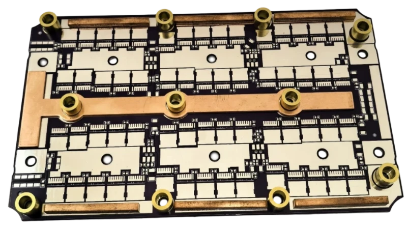
| Copper Weight | 2 oz or higher | Handles high continuous currents and aids thermal dissipation. | Specify in fabrication notes. | Thermal hotspots, trace fusing. |
| Material Tg | > 170°C (High Tg) | SiC runs hot; standard FR4 may delaminate. | Check material datasheet (e.g., Isola 370HR). | PCB delamination, barrel cracks. |
| Symmetry | Match High/Low side | Asymmetry causes timing skew and uneven stress. | Measure path lengths for H-bridge. | Shoot-through risk, uneven thermal load. |
Implementation steps

Once the specifications are understood, the design must be executed methodically. Here is the step-by-step workflow for implementing SiC inverter gate driver PCB best practices.
- Component Placement Strategy
- Action: Place the SiC MOSFETs and the gate driver ICs first.
- Key Parameter: Distance < 20mm.
- Acceptance Check: Verify that the driver output pin faces the MOSFET gate pin directly to avoid meandering traces.
- Kelvin Source Routing
- Action: Route the gate return trace directly to the source pin of the MOSFET, separate from the main power ground plane.
- Key Parameter: Kelvin connection point must be at the pad.
- Acceptance Check: Ensure the "Power Source" and "Driver Source" do not share a path until the MOSFET pin.
- Gate Loop Optimization
- Action: Route the Gate and Return traces on adjacent layers (e.g., Layer 1 and Layer 2) exactly on top of each other.
- Key Parameter: Loop Inductance < 10 nH.
- Acceptance Check: Use a PCB viewer or 3D tool to visualize the loop area; it should look like a line, not a circle.
- Power Loop Minimization
- Action: Place the DC link capacitor as close as possible to the half-bridge to minimize the commutation loop.
- Key Parameter: Bus inductance < 20 nH.
- Acceptance Check: Verify that the positive and negative bus plates overlap heavily to cancel magnetic fields.
- Isolation Barrier Design
- Action: Create a clear "keep-out" zone under the isolation components (optocouplers/transformers). Remove all inner layer copper in this zone.
- Key Parameter: Creepage > 8mm (system dependent).
- Acceptance Check: Run a High-Voltage DRC to ensure no copper infringes on the isolation gap.
- Decoupling Capacitor Layout
- Action: Place C0G/NP0 ceramic capacitors immediately at the VDD/VEE pins of the driver.
- Key Parameter: Trace length to cap < 2mm.
- Acceptance Check: Ensure vias connecting capacitors to ground are doubled or tripled to reduce inductance.
- Thermal Via Stitching
- Action: Place arrays of thermal vias under the exposed pads of the driver and MOSFETs.
- Key Parameter: Via diameter 0.3mm, pitch 0.6mm.
- Acceptance Check: Verify solder mask opening allows for heat dissipation but prevents solder wicking (tenting or plugging may be needed).
- DFM Review for Assembly
- Action: Check component spacing for automated pick-and-place, especially for heavy copper boards.
- Key Parameter: Min component spacing.
- Acceptance Check: Consult DFM guidelines to ensure the design is manufacturable at scale.
Failure modes & troubleshooting
Even with a rigorous design process, issues can arise during testing. Troubleshooting SiC inverter gate driver PCB best practices requires identifying specific symptoms that point to layout flaws.
Symptom: Excessive Ringing on Gate Voltage
- Cause: High parasitic inductance in the gate loop.
- Check: Measure the length of the trace from driver to gate. Check for vias in the gate path.
- Fix: Shorten traces; remove vias if possible. Add a ferrite bead or increase gate resistance ($R_g$) slightly (trade-off with switching speed).
- Prevention: Use stripline routing or microstrip with a ground plane immediately below.
Symptom: False Turn-On (Miller Effect)
- Cause: High dV/dt coupling through the Miller capacitance ($C_{gd}$) raises the gate voltage.
- Check: Look for voltage spikes on the gate of the OFF device when the ON device switches.
- Fix: Implement an Active Miller Clamp or use a negative turn-off voltage (e.g., -5V).
- Prevention: Keep the gate turn-off path impedance extremely low.
Symptom: Driver Latch-Up or Reset
- Cause: Common Mode Transient Immunity (CMTI) violation or ground bounce.
- Check: Verify the isolation rating of the driver. Check ground potential difference between logic and power sides.
- Fix: Add common-mode chokes; improve isolation capacitance.
- Prevention: Select gate drivers with CMTI > 100 kV/µs.
Symptom: MOSFET Overheating (Static)
- Cause: Gate voltage not reaching full saturation (e.g., 15V or 18V) or poor thermal path.
- Check: Measure $V_{gs}$ at the pin. Check thermal via continuity.
- Fix: Increase trace width for power delivery to the driver; improve heatsink attachment.
- Prevention: Use heavy copper (2oz+) and high-performance thermal substrates.
Symptom: EMI/EMC Test Failure
- Cause: Large power commutation loops acting as antennas.
- Check: Analyze the physical area of the DC+ to DC- loop including the switch.
- Fix: Add snubber circuits (RC or RCD); improve shielding.
- Prevention: Laminar busbar design or overlapping PCB power planes.
Symptom: Dielectric Breakdown (Arcing)
- Cause: Insufficient creepage/clearance for the operating altitude or pollution degree.
- Check: Inspect the PCB for carbon tracks or burns across isolation gaps.
- Fix: Mill slots (cutouts) in the PCB to increase creepage distance.
- Prevention: Strictly follow IEC 60664-1 tables during layout.
Design decisions
Troubleshooting often leads back to fundamental design choices made early in the project.
Layer Stackup Selection For SiC inverters, a standard 2-layer board is rarely sufficient due to the need for low inductance.
- 4-Layer Stackup: Signal / Ground / Power / Signal. This is the minimum recommended. The internal ground plane acts as a shield and reduces loop inductance for top-layer traces.
- 6-Layer Stackup: Allows for dedicated shielding layers and better isolation between high-voltage and low-voltage logic.
Material Selection Standard FR4 (Tg 130-140°C) may not survive the thermal cycling of high-power SiC applications.
- High Tg FR4: Materials like Isola 370HR (Tg 180°C) are recommended for reliability.
- Heavy Copper: Using 2oz, 3oz, or even 4oz copper helps with thermal spreading and reducing the resistance of high-current tracks.
Gate Driver Topology
- Isolated vs. Non-Isolated: High-voltage inverters invariably require galvanic isolation (optical, capacitive, or magnetic).
- Bipolar Supply: Using +15V/-5V is a standard design decision to prevent false turn-on, requiring specific power supply layout considerations on the PCB.
FAQ
Q: What is the most critical rule for SiC gate driver layout? A: Minimizing the gate loop inductance is the most critical.
- Keep traces short (<20mm).
- Run gate and return traces parallel and close together.
- Avoid vias in the gate path.
Q: Do I really need negative gate voltage for SiC? A: While some SiC FETs can operate at 0V off, negative voltage (-3V to -5V) is highly recommended.
- It provides a safety margin against Miller effect turn-on.
- It speeds up turn-off times.
Q: Can I use standard FR4 for SiC inverter PCBs? A: It depends on the temperature and voltage.
- For prototypes or lower power, standard FR4 is fine.
- For high-power density or automotive, use High Tg materials to prevent thermal failure.
Q: How do I calculate the required creepage distance? A: Refer to standards like IEC 60664-1.
- Determine the working voltage (e.g., 800V).
- Determine the pollution degree (usually 2 for sealed, 3 for open).
- Select the material group (CTI value).
Q: Why is CMTI important for SiC? A: SiC switches have very fast voltage transients (high dV/dt).
- Low CMTI drivers interpret this noise as a signal.
- This causes glitches or loss of sync.
Q: How does trace width affect the gate driver? A: Thin traces have higher inductance and resistance.
- This limits the peak current the driver can push/pull.
- It slows down switching, increasing switching losses.
Q: Should I use a bead on the gate? A: A ferrite bead can suppress high-frequency ringing.
- It adds resistance at high frequencies without affecting DC drive.
- Place it close to the gate pin.
Q: What is the benefit of Kelvin source connections? A: It bypasses the common source inductance.
- The gate loop does not see the voltage drop caused by the main load current.
- This results in cleaner, faster switching.
Q: How do I verify impedance control on gate traces? A: Use an impedance calculator during design.
- Define the stackup and dielectric constant.
- Adjust trace width to match target impedance (though minimizing inductance is usually prioritized over matching impedance in short runs).
Q: What is the lead time for manufacturing SiC-grade PCBs? A: It varies by complexity and material availability.
- Standard High Tg boards: 3-5 days.
- Heavy copper or specialized substrates: 7-10 days.
Related pages & tools
To further assist with your SiC inverter gate driver PCB best practices, utilize these resources:
- PCB Impedance Calculator: Essential for calculating trace width and spacing to manage inductance and impedance.
- DFM Guidelines: Ensure your layout meets manufacturing constraints to avoid costly redesigns.
- Get a Quote: Ready to manufacture? Upload your Gerber files for a quick cost estimation.
Glossary (key terms)
| Term | Definition | Relevance to SiC PCB |
|---|---|---|
| SiC (Silicon Carbide) | A wide-bandgap semiconductor material allowing higher voltage and faster switching than Silicon. | The core technology requiring specialized PCB layout rules. |
| dV/dt | The rate of change of voltage with respect to time. | High dV/dt in SiC creates noise and requires high CMTI drivers. |
| Parasitic Inductance | Unwanted inductance inherent in PCB traces and component leads. | The primary enemy of fast switching; causes ringing and overshoots. |
| Miller Effect | A phenomenon where capacitance ($C_{gd}$) couples voltage to the gate, potentially turning it on. | Requires negative gate drive or Miller clamps in the PCB design. |
| Kelvin Connection | A 4-wire measurement technique applied to PCB routing to separate force and sense paths. | Critical for isolating the gate return path from high-current power paths. |
| CMTI | Common Mode Transient Immunity; the ability of an isolator to reject fast transient noise. | Must be high (>100 kV/µs) to prevent driver corruption. |
| Desaturation (Desat) | A protection method that detects if the MOSFET is in a short-circuit state. | Requires careful routing of detection traces to avoid false trips. |
| Loop Area | The physical area enclosed by a current path and its return. | Must be minimized to reduce EMI and inductance. |
| Creepage | The shortest distance between two conductive parts along the surface of the insulation. | Critical for high-voltage safety isolation. |
| Clearance | The shortest distance between two conductive parts through the air. | Prevents arcing in high-voltage designs. |
| Gate Resistor ($R_g$) | A resistor placed in series with the gate to control switching speed and damp ringing. | Placement and value selection are key tuning parameters. |
| C0G/NP0 | A type of ceramic capacitor dielectric with high stability. | Recommended for decoupling and timing in harsh thermal environments. |
Conclusion
Implementing SiC inverter gate driver PCB best practices is not just about following a checklist; it is about respecting the physics of high-speed, high-voltage switching. By minimizing loop inductance, ensuring robust isolation, and selecting the right materials, you can unlock the full efficiency potential of Silicon Carbide technology without sacrificing reliability.
Whether you are prototyping a new EV traction inverter or optimizing an industrial power supply, the layout is the foundation of your success. APTPCB specializes in manufacturing high-performance PCBs that meet these rigorous demands. If you have your design ready or need advice on material selection for your next SiC project, reach out to us for a manufacturing assessment.