Silicon carbide MOSFET gate drivers enable ultra-fast switching (10-100ns rise/fall times), high-temperature operation (175-200°C junction), and superior efficiency unlocking next-generation electric vehicle powertrains, DC fast chargers, and compact industrial drives operating at 20-100kHz+ switching frequencies achieving >99% efficiency and 5-10x higher power density compared to silicon IGBTs with successful operation through millions of rapid switching cycles over 15-20 year service lives.
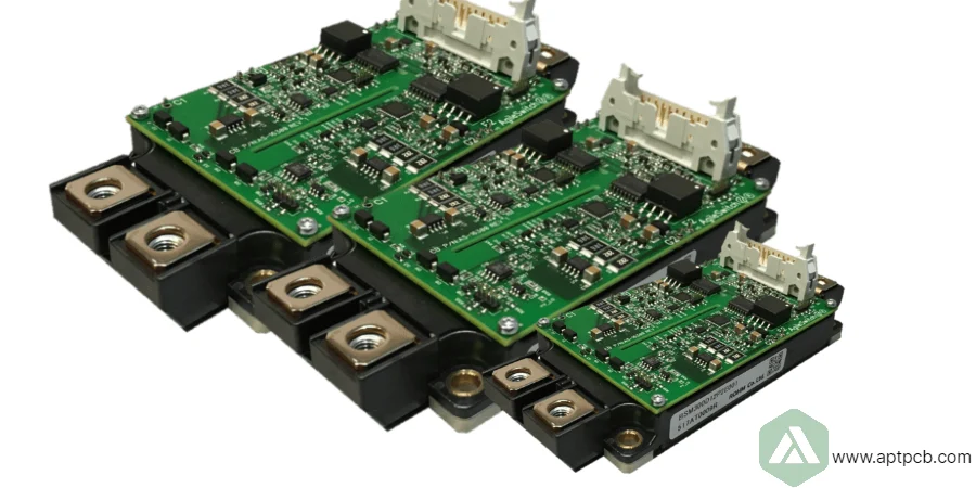
At APTPCB, we manufacture SiC gate driver PCBs with aerospace defense grade processes implementing ultra-low inductance layouts, negative gate voltage drives, and advanced protection features. Our capabilities support SiC MOSFETs from 650V fast chargers through 1700V traction inverters across currents from 100A through 800A+ with comprehensive high-frequency characterization.
Managing Ultra-Fast Switching
SiC MOSFETs switch 5-10x faster than silicon IGBTs achieving 10-50ns rise times enabling 50-100kHz switching reducing magnetic component size and weight. However, ultra-fast switching creates challenges: sub-nanohenry parasitic inductance causes excessive ringing and voltage overshoot; gate drive circuits require multi-ampere peak currents; electromagnetic interference increases requiring careful PCB layout and shielding; and measurement equipment must capture nanosecond-scale transients during characterization and production testing.
At APTPCB, our PCB manufacturing implements ultra-low inductance layouts supporting SiC switching speeds.
Key Fast Switching Requirements
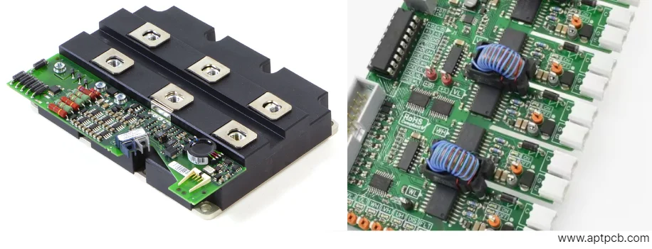
Ultra-Low Inductance Layout
- Gate drive loop inductance <5nH minimizing ringing and overshoot during transitions with medical devices quality assembly precision
- Power loop inductance <10nH reducing voltage spikes during current commutation
- Kelvin source connection separating gate drive current from main source current eliminating shared inductance
- Wide, short traces in gate circuit minimizing resistive and inductive impedance
- Multi-layer PCB with power planes providing low-inductance current return paths
- Component placement optimization keeping gate driver IC within 5-10mm of SiC MOSFET
High Peak Gate Current
- Gate driver ICs sourcing/sinking 5-10A peak rapidly charging Qg (typically 100-300nC)
- Low output impedance driver maintaining voltage during peak current delivery
- Adequate gate supply decoupling providing instantaneous charge without voltage sag
- PCB copper weight and width handling brief high current pulses without voltage drop
- Thermal management of gate drivers and resistors dissipating power at high switching frequencies
- Driver IC selection balancing current capability against propagation delay and power consumption
EMI Management
- Controlled switching speed balancing losses against EMI generation using gate resistance optimization
- Common-mode choke filtering reducing conducted EMI on gate drive power supplies
- Shielding and grounding preventing radiated emissions from high di/dt and dv/dt paths
- Spread spectrum modulation randomizing switching frequency reducing peak EMI amplitudes
- Multi-layer PCB construction providing grounding and shielding layers
- Pre-compliance EMI testing during development identifying issues before formal certification
Implementing Negative Gate Voltage
SiC MOSFETs benefit from negative gate voltage (-2 to -5V) during off-state providing superior immunity to parasitic turn-on from high dv/dt (>50V/ns) common in SiC applications. Negative voltage also accelerates turn-off, reduces switching losses, and provides robustness against Miller effect. However, negative supply implementation adds complexity requiring dual supplies, proper sequencing, and protection against excessive negative voltage damaging gate oxide.
APTPCB implements robust negative gate voltage supplies supporting SiC operation.
Key Negative Voltage Implementation
Negative Supply Generation
- Charge pump circuits generating -2 to -5V from positive supply with server data center reliability requirements
- Isolated DC-DC converters providing dual ±15V supplies powering gate drivers
- Bootstrap methods in cost-sensitive applications combining positive and negative rails
- Supply sequencing ensuring proper power-up and power-down sequences
- Voltage regulation maintaining negative voltage accuracy across load variations
- Over-voltage protection preventing excessive negative voltage damaging SiC gates
Gate Drive Voltage Optimization
- Positive voltage selection (+15 to +20V) balancing turn-on speed against gate oxide stress
- Negative voltage selection (-2 to -5V) optimizing turn-off performance and dv/dt immunity
- Active gate drive control dynamically adjusting voltages based on operating conditions
- Temperature compensation maintaining performance across -40 to +150°C ambient
- Split supply architecture enabling independent positive and negative voltage adjustment
- Comprehensive testing validating gate drive performance across operating envelope
Managing High-Temperature Operation
SiC devices operate at 175-200°C junction temperatures requiring gate drive circuits surviving elevated ambient temperatures while maintaining performance and reliability. High-temperature operation stresses passive components, solder joints, PCB materials, and semiconductor devices requiring careful material selection, thermal management, and validated qualification testing ensuring 10-15 year operational lifetime despite continuous exposure to elevated temperatures.
APTPCB implements high-temperature capable gate driver assemblies.
Key High-Temperature Design Requirements
Component Selection
- High-temperature rated ICs (125-150°C junction) surviving elevated ambient
- Ceramic capacitors maintaining characteristics across temperature (X7R, X5R dielectrics)
- Film resistors with stable resistance and low tempco across operating range
- High-temperature solder (SAC305 or high-temp alternatives) maintaining joint integrity
- Gate driver ICs rated for automotive or industrial temperature ranges
- Security equipment grade qualification ensuring long-term reliability
Thermal Management
- Heat spreading through heavy copper or aluminum core PCBs
- Thermal vias transferring heat from components to heat sinks
- Adequate spacing preventing thermal coupling between heat-generating devices
- Thermal simulation predicting temperatures validating designs before prototyping
- Active cooling when required using forced air or liquid cooling
- Temperature sensors enabling thermal monitoring and protection
Providing Advanced Protection Features
SiC MOSFETs require enhanced protection compared to silicon IGBTs due to smaller die sizes, faster switching, and higher operating temperatures. Protection circuits must detect faults within nanoseconds, provide coordinated shutdown preventing secondary failures, and enable diagnostics supporting field troubleshooting. Advanced protection implementations combine hardware circuits for immediate response with software monitoring enabling predictive maintenance and optimization.
APTPCB implements comprehensive SiC protection circuits.
Key Protection Requirements
Overcurrent and Short Circuit Protection
- Drain-source voltage monitoring detecting desaturation indicating overcurrent
- di/dt sensing detecting excessive current rise rate indicating short circuit
- Fast response (<100ns) initiating soft turn-off before thermal damage
- Current limiting reducing gate voltage during overcurrent maintaining partial conduction
- Fault reporting communicating protection events to system controller
- Multiple protection layers providing redundancy ensuring safe operation
Overvoltage and Undervoltage Protection
- Drain voltage monitoring preventing operation beyond rated voltage
- Gate supply monitoring ensuring adequate voltage for proper switching
- Transient suppression limiting voltage spikes from stray inductance
- Avalanche protection preventing excessive energy dissipation during voltage spikes
- Coordinated protection between multiple devices in parallel or series operation
- Diagnostic capabilities identifying failure modes supporting troubleshooting
Optimizing for EV and Fast Charging Applications
Electric vehicles represent primary SiC adoption market requiring gate drivers optimized for automotive environment, functional safety standards, high-volume manufacturing, and cost targets. EV traction inverters operate at 400-800V, 200-500kW handling acceleration, regenerative braking, and continuous highway operation. DC fast chargers transfer 50-350kW requiring reliable operation in roadside locations with varying power quality and environmental conditions.
APTPCB supports EV manufacturers with automotive-qualified SiC gate driver manufacturing.
Key EV Application Requirements
Automotive Qualification
- AEC-Q100/200 qualified components surviving automotive temperature, vibration, and lifetime
- Functional safety (ISO 26262 ASIL-C/D) ensuring safe operation despite single-point failures
- Automotive EMC compliance meeting stringent emission and immunity requirements
- High-voltage safety standards compliance protecting occupants from electrical hazards
- Production part approval process (PPAP) documentation supporting automotive supply chain
- Long-term supply commitment matching automotive program lifecycles (10-15 years)
Performance Optimization
- High efficiency (>99%) maximizing vehicle range and reducing cooling requirements
- Compact design fitting within space-constrained vehicle powertrain packaging
- Acoustic noise optimization minimizing audible switching frequencies
- Thermal management surviving underhood temperatures and transient heat loads
- Reliability targets matching automotive expectations (15-20 year life, 200k+ miles)
- Cost optimization achieving automotive industry pricing targets through volume manufacturing
Through automotive-qualified processes, high-volume manufacturing capabilities, and comprehensive engineering support, APTPCB enables EV manufacturers deploying next-generation SiC-based powertrains achieving superior efficiency, performance, and packaging compared to silicon alternatives.