High-efficiency power conversion relies heavily on Silicon Carbide (SiC) technology, but the performance of these components is strictly limited by the physical design of the PCB. A poor SiC rectifier board layout can turn a high-performance semiconductor into a source of dangerous voltage spikes, excessive electromagnetic interference (EMI), and thermal failure. Unlike standard silicon-based designs, SiC devices switch at incredibly high speeds (high dV/dt and di/dt), meaning that parasitic inductance and capacitance in the board layout are no longer negligible factors—they are critical design constraints.
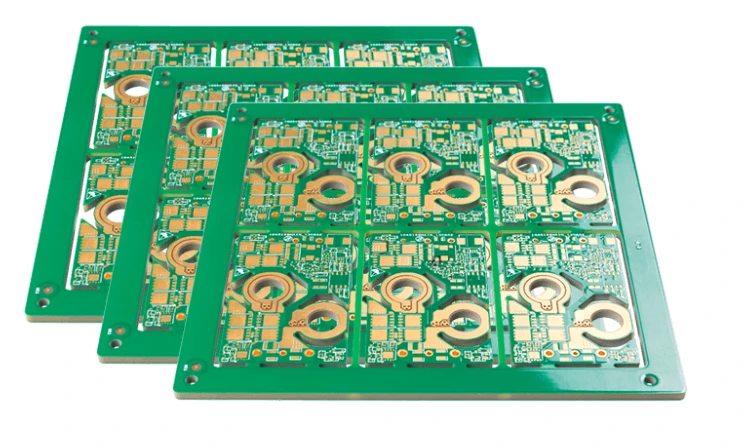
This guide provides a comprehensive technical framework for engineers designing SiC rectifier circuits. We cover the essential specifications, step-by-step implementation strategies, and detailed troubleshooting protocols to ensure your design meets industrial reliability standards. Whether you are prototyping a solar inverter or finalizing an EV charger module, APTPCB (APTPCB PCB Factory) provides the manufacturing precision required to execute these demanding layouts.
Quick Answer (30 seconds)
Successful SiC rectifier board layout requires minimizing the power loop area to reduce parasitic inductance, which causes voltage overshoot and ringing.
- Minimize Loop Inductance: Keep the total loop inductance below 10 nH by placing decoupling capacitors as close as possible to the SiC devices.
- Kelvin Connections: Always use Kelvin source connections for gate driving to decouple the control loop from the power loop.
- Thermal Management: Use heavy copper (2oz or 3oz) and thermal via arrays to manage the high power density of SiC components.
- Gate Drive Proximity: Place the gate driver IC within 20mm of the SiC MOSFET/Diode to reduce gate loop inductance.
- Clearance Rules: Adhere strictly to IPC-2221B voltage clearance standards, as SiC often operates at 600V–1200V+.
- Symmetrical Layout: Ensure symmetrical routing for parallel devices to prevent current imbalance and thermal runaway.
When SiC rectifier board layout applies (and when it doesn’t)
Understanding when to apply specialized SiC layout techniques ensures engineering resources are allocated correctly. SiC requires a different approach than standard Silicon (Si) designs due to its switching speed.
Applies to:
- High-Voltage Systems: Designs operating above 400V (e.g., EV chargers, industrial motor drives) where SiC breakdown voltage is advantageous.
- High-Frequency Switching: Converters operating above 50kHz–100kHz where the switching losses of standard Silicon would be prohibitive.
- High-Temperature Environments: Applications requiring operation above 150°C, leveraging SiC’s thermal stability.
- Space-Constrained Designs: Projects requiring high power density where passive components (inductors/capacitors) must be minimized through high-frequency operation.
- High-Efficiency Requirements: Systems targeting >98% efficiency (e.g., 80 Plus Titanium power supplies).
Does not apply (or is overkill) for:
- Low-Voltage Rectification: Standard 12V/24V AC-DC adapters where Schottky diodes or synchronous Si MOSFETs are sufficient and cheaper.
- Mains Frequency Rectification: 50Hz/60Hz bridge rectifiers where switching speed is negligible, and standard diode bridges are robust enough.
- Cost-Sensitive Consumer Electronics: Low-power devices where the premium cost of SiC components and specialized PCB manufacturing is not justified.
- Legacy Linear Power Supplies: Designs that do not utilize switching topologies.
Rules & specifications
The following table outlines the critical design rules for SiC rectifier board layout. These specifications are derived from best practices in high-voltage power electronics and DFM (Design for Manufacturing) standards.
| Rule | Recommended Value/Range | Why it matters | How to verify | If ignored |
|---|---|---|---|---|
| Power Loop Inductance | < 10 nH (Target < 5 nH) | High di/dt causes voltage spikes ($V = L \cdot di/dt$). Excess inductance leads to device overvoltage. | 3D Field Solver / Q3D Extractor simulation. | Voltage overshoot destroys SiC device; excessive ringing. |
| Gate Loop Inductance | < 20 nH | High inductance slows switching and causes gate ringing, risking false triggering. | Measure trace length; ensure driver is < 20mm from gate. | False turn-on (shoot-through); increased switching losses. |
| Creepage Distance | Per IPC-2221B (e.g., >5mm for 600V) | Prevents surface arcing between high-voltage nodes, especially in dirty environments. | CAD DRC (Design Rule Check) with voltage rules set. | Arcing, carbonization of PCB, catastrophic short circuit. |
| Clearance Distance | Per IPC-2221B (e.g., >3mm for 600V) | Prevents air breakdown between conductive parts. | CAD DRC; check component lead spacing. | Flashover, safety hazard, device failure. |
| Copper Weight | 2 oz, 3 oz, or Heavy Copper | SiC handles high current density; thin copper causes resistive heating ($I^2R$). | Check stackup specification in PCB manufacturing notes. | Trace overheating, delamination, voltage drop. |
| Thermal Via Pitch | 1.0mm - 1.2mm grid | Efficiently transfers heat from the top layer component to inner/bottom ground planes. | Visual inspection of footprint; thermal simulation. | Component overheating, reduced lifespan. |
| Gate Trace Width | > 20 mils (0.5mm) | Reduces trace inductance and resistance for the high peak currents (2A-5A) of gate drivers. | CAD constraints manager. | Slow switching, increased switching loss. |
| Differential Gate Routing | Parallel, tight coupling | Rejects common-mode noise induced by high dV/dt switching events. | Visual check; ensure Gate and Source return run together. | Gate oscillation, unintended switching. |
| Decoupling Cap Placement | < 5mm from device pins | Provides immediate current for switching events, minimizing loop area. | Visual placement check during layout. | High voltage spikes, EMI failures. |
| Layer Stackup | Symmetrical (e.g., 4 or 6 layers) | Prevents board warping during reflow; allows for dedicated ground planes for shielding. | Review stackup with DFM guidelines. | Board warpage, poor EMI performance. |
| Solder Mask Opening | 1:1 or slightly larger | Ensures solder paste release for large pads; prevents solder mask on pads. | Gerber viewer inspection. | Poor solder joints, thermal impedance increase. |
| Component Spacing | > 1mm between HV parts | Prevents thermal coupling and allows for conformal coating flow if needed. | Assembly drawing review. | Thermal hotspots, coating voids. |
Implementation steps

Executing a robust SiC rectifier board layout requires a disciplined workflow. Following these steps ensures that electrical, thermal, and mechanical requirements are met simultaneously.
Step 1: Stackup and Material Selection
- Action: Select a PCB material with a high Tg (Glass Transition Temperature) and appropriate CTI (Comparative Tracking Index).
- Key Parameter: Tg > 170°C; CTI > 600V (PLC 0) for high voltage.
- Acceptance Check: Confirm material availability with APTPCB before starting layout. Standard FR4 may be insufficient for very high voltages; consider materials listed in our PCB materials guide.
Step 2: Component Placement (The Critical Loop)
- Action: Place the SiC diodes/MOSFETs and the DC link capacitor first. These form the high-frequency power loop.
- Key Parameter: Distance between DC link cap terminals and SiC device terminals must be minimized.
- Acceptance Check: The physical loop area should be visible as a tight circle, not a sprawling path.
Step 3: Gate Driver Placement
- Action: Place the gate driver IC immediately next to the SiC switch.
- Key Parameter: Gate trace length < 20mm.
- Acceptance Check: Verify that the gate drive output and the Kelvin source return path run parallel to each other (differential pair routing).
Step 4: Power Plane Definition
- Action: Define large copper pours for the DC+ and DC- rails. Avoid thin traces for power paths.
- Key Parameter: Current density < 30 A/mm² (for temperature rise control).
- Acceptance Check: Use a calculator to verify trace width vs. current capability.
Step 5: Thermal Via Stitching
- Action: Place a grid of thermal vias under the exposed pads of the SiC devices.
- Key Parameter: 0.3mm hole size, 1.0mm pitch, plated shut or tented if required by assembly.
- Acceptance Check: Ensure vias connect to large internal or bottom copper planes for heat spreading.
Step 6: High-Voltage Isolation Cuts
- Action: Add routing keep-out zones and physical slots (milling) between high-voltage nodes if creepage distance on the surface is insufficient.
- Key Parameter: Slot width > 1mm usually adds significant creepage margin.
- Acceptance Check: Run a 3D clearance check in your CAD software.
Step 7: Parasitic Extraction & Simulation
- Action: If available, use simulation tools to extract the loop inductance.
- Key Parameter: Total loop inductance < 10nH.
- Acceptance Check: If inductance is high, move capacitors closer or use a laminated busbar approach within the PCB layers.
Step 8: DFM and Assembly Review
- Action: Check for acid traps, slivers, and solder mask bridges.
- Key Parameter: Minimum solder dam width (usually 4 mils).
- Acceptance Check: Upload files to a Gerber viewer to verify the final manufacturing data matches the design intent.
Failure modes & troubleshooting
Even with a careful SiC rectifier board layout, issues can arise during testing. The high switching speeds of SiC expose weaknesses that standard silicon would hide.
1. Excessive Voltage Overshoot (Ringing)
- Symptom: Voltage spikes across the SiC device exceed the breakdown voltage rating during turn-off.
- Causes: High parasitic inductance in the power loop; insufficient decoupling.
- Checks: Measure the distance between the DC link capacitor and the switch. Check for long, thin traces in the power path.
- Fix: Add high-frequency ceramic (C0G/NP0) snubber capacitors directly across the SiC device pins.
- Prevention: Redesign layout to minimize the physical area of the commutation loop.
2. False Turn-On (Miller Effect)
- Symptom: Shoot-through current; device overheating; unexpected conduction.
- Causes: High dV/dt coupling through the Miller capacitance ($C_{gd}$) lifts the gate voltage. High inductance in the gate return path.
- Checks: Verify if an active Miller clamp is used. Check gate trace impedance.
- Fix: Use a negative gate drive voltage (e.g., -4V or -5V) to provide margin. Reduce gate resistance ($R_g$).
- Prevention: Use Kelvin source connections strictly. Keep the gate driver extremely close to the device.
3. EMI / EMC Failure
- Symptom: Failing radiated or conducted emissions tests.
- Causes: Large switching loops acting as antennas; fast switching edges (high dV/dt) generating high-frequency noise.
- Checks: Identify the "hot" nodes (nodes with high dV/dt) and check their surface area.
- Fix: Add shielding cans; slow down switching speed (increase $R_g$) at the cost of efficiency; add common-mode chokes.
- Prevention: Minimize the copper area of high dV/dt nodes (switched nodes) while maintaining current capacity. Use internal ground planes as shields.
4. Thermal Runaway
- Symptom: Device temperature rises uncontrollably until destruction.
- Causes: Poor thermal interface; insufficient copper weight; lack of thermal vias.
- Checks: Inspect solder voiding on the thermal pad (X-ray). Verify thermal via connectivity.
- Fix: Improve cooling (heatsink, fan).
- Prevention: Use 2oz or 3oz copper. Maximize the number of thermal vias. Ensure the PCB assembly process achieves <25% voiding on large pads.
5. Gate Oxide Breakdown
- Symptom: Permanent short between Gate and Source.
- Causes: Voltage spikes on the gate induced by power loop coupling or ESD.
- Checks: Check for Zener diodes protecting the gate.
- Fix: Install bidirectional TVS diodes close to the gate-source pins.
- Prevention: Tight coupling of gate and source traces (differential routing) to reject induced noise.
6. Solder Joint Fatigue
- Symptom: Intermittent operation or open circuits after thermal cycling.
- Causes: CTE (Coefficient of Thermal Expansion) mismatch between the ceramic SiC package and the FR4 PCB.
- Checks: Inspect joints for cracks.
- Fix: Use underfill or flexible solder alloys.
- Prevention: Choose PCB materials with CTE matched closer to the component, or use leaded packages for stress relief.
Design decisions
When planning a SiC rectifier board layout, several strategic decisions must be made early in the process. These choices dictate the cost, performance, and manufacturability of the final board.
Material Selection: FR4 vs. Specialized Substrates Standard FR4 is cost-effective but has limitations in thermal conductivity and high-frequency loss. For high-power SiC applications, engineers often consider:
- High-Tg FR4: Essential for lead-free soldering and high operating temperatures.
- Ceramic Substrates (DBC): Used for extremely high power modules, offering superior thermal performance but at a much higher cost.
- Metal Core PCB (MCPCB): Excellent for heat dissipation but generally limited to single-layer routing, making low-inductance layout difficult.
- Decision Guide: Use High-Tg FR4 with heavy copper for most <10kW designs. Consider IMS/MCPCB only if the topology allows for simple routing.
Copper Thickness: 1oz vs. Heavy Copper SiC devices are small but handle massive power.
- 1oz (35µm): Generally insufficient for the main power path in SiC designs unless traces are extremely wide.
- 2oz - 3oz (70µm - 105µm): The standard for power electronics. Allows for narrower traces (reducing inductance) while handling current.
- Decision Guide: Start with 2oz copper. If thermal simulation shows hotspots, move to 3oz or add busbars.
Surface Finish
- HASL (Hot Air Solder Leveling): Not recommended for fine-pitch SiC packages due to uneven surfaces.
- ENIG (Electroless Nickel Immersion Gold): Excellent flatness, good for wire bonding and fine pitch.
- Immersion Silver: Good conductivity but sensitive to tarnishing.
- Decision Guide: Choose ENIG for the best balance of flatness, solderability, and reliability in high-value SiC boards.
Gate Drive Topology
- Unipolar (0V to 15V): Simpler, but risks false turn-on due to Miller effect.
- Bipolar (-4V to 15V): Requires a more complex power supply but provides robust immunity against false triggering.
- Decision Guide: Always use Bipolar gate drive for SiC designs >600V or hard-switching topologies.
FAQ
Q: Why is loop inductance more critical in SiC than in Silicon IGBTs? A: SiC devices switch 10x to 100x faster than IGBTs. The voltage spike generated is proportional to switching speed ($di/dt$). Even 10nH of inductance can generate destructive voltage spikes at SiC speeds, whereas an IGBT might tolerate it.
- SiC $di/dt$ can exceed 3000 A/µs.
- IGBT $di/dt$ is typically < 500 A/µs.
Q: Can I use standard FR4 for SiC rectifier boards? A: Yes, but with caveats. You must use High-Tg FR4 (Tg > 170°C) to withstand the higher operating temperatures. For voltages >1000V, pay close attention to the CTI rating of the laminate to prevent tracking.
Q: What is the Kelvin connection and why is it mandatory? A: A Kelvin connection separates the high-current power path from the sensitive control (gate) path.
- It prevents the voltage drop across the source inductance from subtracting from the gate drive voltage.
- Without it, switching slows down, and oscillation occurs.
Q: How do I handle heat if the SiC device is Surface Mount (SMD)? A: You must rely on the PCB for cooling.
- Use a dense array of thermal vias (0.3mm hole, 1mm pitch) under the thermal pad.
- Connect these vias to large copper planes on inner and bottom layers.
- Attach a heatsink to the bottom of the PCB using a thermal interface material (TIM).
Q: What is the recommended gate trace width? A: While the average gate current is low, the peak current is high (often 2A–5A).
- Use traces at least 20 mils (0.5mm) wide.
- Keep length under 20mm.
- Minimize vias in the gate path (vias add inductance).
Q: Should I use a ground plane for SiC layouts? A: Yes, but be careful.
- Do not put a ground plane directly under the high-voltage switching node (drain/collector) if possible, as this creates parasitic capacitance ($C_{oss}$) which increases switching losses.
- Do use ground planes under the low-voltage control circuitry to shield it from noise.
Q: How does APTPCB ensure the reliability of SiC boards? A: We utilize automated optical inspection (AOI) and E-testing to verify connectivity. For high-voltage boards, we can perform specific impedance control checks and ensure material specs (like heavy copper adhesion) meet IPC Class 2 or 3 standards.
Q: What is the impact of "acid traps" in high-voltage layouts? A: Acid traps (acute angles in traces) can retain etchant, causing corrosion over time. In high-voltage SiC boards, this corrosion can lead to open circuits or, worse, create a path for arcing. Always use 45-degree angles, never 90-degree or acute angles.
Q: How do I calculate the required creepage for 1200V SiC? A: Refer to IPC-2221B.
- For uncoated external conductors: ~6mm to 10mm depending on pollution degree.
- Using a slot (milling) between pads can effectively increase the creepage distance without moving components further apart.
Q: What is the best way to test a prototype SiC board? A: Start with low voltage (e.g., 50V) and verify gate signals.
- Use a high-bandwidth oscilloscope (>500MHz) and high-voltage differential probes.
- Standard passive probes will load the circuit and give false waveforms.
- Slowly increase bus voltage while monitoring for ringing.
Glossary (key terms)
| Term | Definition |
|---|---|
| SiC (Silicon Carbide) | A wide-bandgap semiconductor material allowing higher voltage, temperature, and switching frequency than Silicon. |
| Parasitic Inductance | Unwanted inductance inherent in PCB traces and component leads that resists change in current. |
| dV/dt | The rate of change of voltage over time. High dV/dt in SiC causes noise coupling and EMI. |
| di/dt | The rate of change of current over time. High di/dt generates voltage spikes across inductances. |
| Kelvin Connection | A layout technique using separate pairs of contacts for current carrying and voltage sensing (or gating) to eliminate interference. |
| Miller Effect | The increase in equivalent input capacitance due to amplification of capacitance between input and output terminals ($C_{gd}$). |
| Loop Area | The physical area enclosed by the current path. Larger area = higher inductance = worse performance. |
| Creepage | The shortest distance between two conductive parts along the surface of the insulation material. |
| Clearance | The shortest distance between two conductive parts through the air. |
| CTI (Comparative Tracking Index) | A measure of the electrical breakdown (tracking) properties of an insulating material. |
| Thermal Via | A plated hole used specifically to conduct heat from one layer of the PCB to another, rather than just electrical signals. |
| Commutation Loop | The path current takes during the transition from the switch conducting to the diode conducting (and vice versa). |
Conclusion
Designing a SiC rectifier board layout is a balancing act between minimizing parasitic inductance, managing intense thermal loads, and adhering to high-voltage safety rules. The difference between a reliable power module and a failed prototype often lies in the details: the tightness of the commutation loop, the symmetry of the routing, and the quality of the PCB substrate.
By following the specifications and troubleshooting steps outlined above, you can harness the full potential of Silicon Carbide technology. When you are ready to turn your layout into a physical reality, APTPCB is ready to assist. Our manufacturing capabilities are optimized for the heavy copper, high-Tg, and precision tolerance requirements of modern power electronics.
Submit your Gerber files today for a comprehensive DFM review and ensure your SiC design is built to perform.