Definition, scope, and who this guide is for
Single layer PCBs represent the foundational tier of printed circuit board manufacturing, characterized by having conductive copper circuitry on only one side of the substrate. While often perceived as "low-tech," mastering single layer pcb basics is critical for procurement leads and engineers managing high-volume consumer electronics, power supplies, and LED lighting projects where cost efficiency and thermal management are paramount. Unlike multi-layer boards that rely on complex internal vias and lamination cycles, single layer boards rely heavily on material properties and precise surface processing to ensure reliability.
This guide is designed for technical buyers, product engineers, and supply chain managers who need to source single layer boards without compromising quality. It moves beyond general definitions to cover the specific procurement specifications, risk mitigation strategies, and validation protocols required to scale production. Whether you are transitioning a prototype to mass production or optimizing an existing BOM, understanding these basics ensures you ask the right questions before issuing a purchase order.
At APTPCB (APTPCB PCB Factory), we often see that the simplest designs suffer the most avoidable failures due to vague documentation or mismatched material selection. This playbook provides a structured approach to defining your requirements, validating supplier capabilities, and ensuring that your single layer designs meet the rigorous demands of modern assembly lines.
When to use single layer pcb basics (and when a standard approach is better)
Understanding the operational context is the first step in applying single layer pcb basics effectively; knowing when to opt for this architecture saves significant costs, but misapplication leads to field failures.
Use Single Layer PCBs When:
- Cost is the Primary Driver: For high-volume consumer goods (calculators, remote controls, simple toys), the reduced material and processing costs of single-sided boards are unbeatable.
- Circuit Complexity is Low: If the schematic allows for routing without crossing traces (or can utilize simple jumper wires), a single layer is sufficient.
- Thermal Dissipation is Critical: In LED lighting and power conversion, single layer Metal Core PCBs (MCPCBs) offer superior heat transfer because the dielectric is directly bonded to a metal heatsink without intervening glass-epoxy layers.
- Manufacturing Speed is Required: With fewer process steps (no lamination, often no plating), throughput is faster.
Switch to Double-Sided or Multi-Layer When:
- Density Requires Fine Pitch: If you need tight component placement basics for BGAs or high-pin-count ICs, single layer routing becomes impossible.
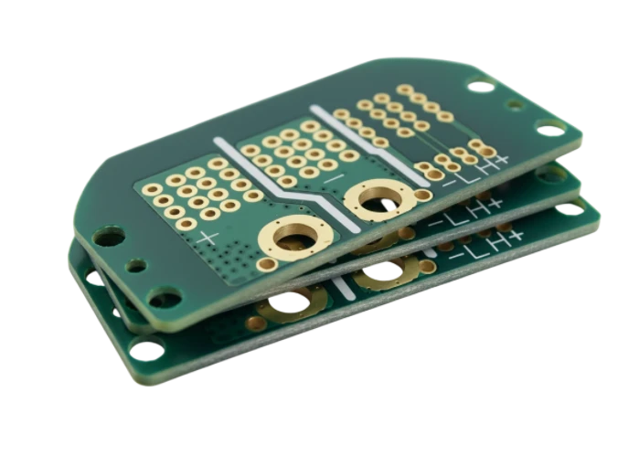
- Mechanical Strength of Through-Holes is Needed: Single layer boards typically use Non-Plated Through Holes (NPTH). If components are heavy or subject to vibration, the lack of a plated barrel reduces solder joint strength significantly compared to Plated Through Holes (PTH) found in double-sided boards.
- Signal Integrity is a Priority: Single layer boards lack reference planes (ground/power planes), making them unsuitable for high-speed digital signals or sensitive RF circuits due to EMI susceptibility.
single layer pcb basics specifications (materials, stackup, tolerances)
Defining precise specifications upfront prevents the "assumption gap" where suppliers default to the cheapest options; here are the critical parameters to define for single layer pcb basics.
- Base Material (Substrate):
- FR-4: The standard glass-reinforced epoxy. Specify Tg (Glass Transition Temperature) typically 130°C–140°C for general use. See FR4 PCB for details on high-Tg options.
- CEM-1 / CEM-3: Composite materials (paper core with glass surface). Cheaper than FR-4 and punchable, making them ideal for mass production of simple shapes.
- Aluminum/Copper Core: Essential for LED/Power apps. Specify thermal conductivity (e.g., 1.0 W/mK to 3.0 W/mK).
- Copper Weight:
- Standard: 1 oz (35µm).
- Power Applications: 2 oz (70µm) or 3 oz (105µm). Note that heavier copper requires wider minimum trace widths/spacing (etching compensation).
- Board Thickness:
- Standard: 1.6mm (0.062").
- Thin options: 0.8mm, 1.0mm, 1.2mm (often used to save cost or space).
- Tolerance: Typically ±10% for FR-4; ±0.1mm for punched boards.
- Surface Finish:
- OSP (Organic Solderability Preservative): Lowest cost, flat surface, good for SMT. Shelf life is short (6 months).
- HASL (Hot Air Solder Leveling): Robust, long shelf life, but surface unevenness can affect fine-pitch SMT.
- ENIG (Electroless Nickel Immersion Gold): Flat, oxidation resistant, expensive. Use for wire bonding or touch contacts.
- Solder Mask:
- Color: Green is standard (best performance/cost). White is common for LEDs (reflectivity).
- Clearance: Minimum 2-3 mil larger than pad size (LDI) or 4-5 mil (traditional photo).
- Silkscreen:
- White or Black. Ensure character height is at least 30-40 mil for legibility.
- Hole Type:
- NPTH (Non-Plated Through Hole): The standard for single layer.
- Tolerance: ±0.05mm (drilled), ±0.10mm (punched).
- Trace/Space:
- Standard: 6/6 mil (0.15mm).
- Advanced: 4/4 mil (0.1mm) – costs increase.
- Bow and Twist:
- Target < 0.75% (IPC Class 2). Single layer boards are prone to warping due to asymmetric copper loading.
- Documentation:
- Adhere to pcb documentation basics: Gerber RS-274X format, Drill file (Excellon), and a ReadMe text file specifying the stackup and finish.
single layer pcb basics manufacturing risks (root causes and prevention)
Even simple designs have failure modes; understanding these risks within the context of single layer pcb basics allows you to implement early detection and prevention strategies.
- Board Warpage (Bow and Twist)
- Root Cause: Asymmetric stackup. Copper is only on one side, creating uneven thermal expansion/contraction during reflow and manufacturing.
- Detection: Visual inspection on a flat granite surface; measurement with feeler gauges.
- Prevention: Use stiffer material (FR-4 over CEM-1) if possible; use copper balancing (thieving) on the etch side to distribute stress evenly; use fixtures during reflow.
- Pad Peeling / Lifted Pads
- Root Cause: Single layer boards rely solely on the adhesive bond between the copper foil and the substrate. There is no plated barrel to anchor the pad. Excessive heat during soldering or mechanical stress lifts the pad.
- Detection: Peel strength testing on test coupons; visual inspection after rework simulation.
- Prevention: Maximize pad size (annular ring); use teardrops at trace-to-pad junctions; specify high-peel-strength laminates; avoid heavy components without mechanical support (glue/screws).
- Solder Mask Misalignment
- Root Cause: Material shrinkage/stretching during processing, especially with cheaper substrates like CEM-1.
- Detection: Visual inspection; check if mask encroaches on solderable pads (solder skip risk).
- Prevention: Use LDI (Laser Direct Imaging) for tighter registration; ensure gerber file basics include adequate mask expansion (dam size).
- Poor Solderability (Black Pad or Oxidation)
- Root Cause: Expired OSP finish or poor HASL process control.
- Detection: Wetting balance test; visual inspection of non-wetting during assembly.
- Prevention: Enforce strict shelf-life controls; vacuum packaging with desiccant; choose ENIG for long storage needs.
- Punching Cracks (CEM-1/FR-1)
- Root Cause: Dull punch tools or improper temperature during the punching process causes haloing or cracks around holes.
- Detection: Backlight inspection; cross-sectioning.
- Prevention: Regular tool maintenance schedules at the supplier; specify drilled holes for critical FR-4 boards instead of punching.
- Clearance Failures (High Voltage)
- Root Cause: Insufficient spacing between traces for the operating voltage, leading to arcing (creepage).
- Detection: Hi-Pot testing (Electrical Safety Compliance).
- Prevention: Follow clearance and creepage basics (IPC-2221 standards); add slots (routing) between high-voltage nodes to increase creepage distance.
- Scratched Circuitry
- Root Cause: Handling damage. Since circuitry is exposed on the bottom side without internal protection, it is vulnerable.
- Detection: AOI (Automated Optical Inspection).
- Prevention: Proper racking and handling protocols; protective coating (conformal coating) post-assembly.
- Incomplete Etching (Shorts)
- Root Cause: Under-etching leaves residual copper between tight traces.
- Detection: E-Test (Electrical Test) – Open/Short test.
- Prevention: Design for Manufacturing (DFM) review to ensure spacing matches copper weight (e.g., don't try 4mil space with 2oz copper).
single layer pcb basics validation and acceptance (tests and pass criteria)

To ensure the delivered product meets the single layer pcb basics requirements, implement a validation plan that moves beyond simple visual checks.
- Electrical Continuity & Isolation (E-Test):
- Objective: Verify no opens or shorts.
- Method: Flying probe (for prototypes) or Bed of Nails (for mass production).
- Acceptance: 100% Pass. No resistance > 10 ohms (continuity) or < 10 M-ohms (isolation).
- Solderability Test:
- Objective: Ensure pads accept solder during assembly.
- Method: IPC-J-STD-003 (Dip and Look).
- Acceptance: >95% coverage of the pad surface with a smooth, continuous solder coating.
- Peel Strength Test:
- Objective: Verify copper adhesion to the substrate.
- Method: IPC-TM-650 2.4.8.
- Acceptance: > 1.1 N/mm (or as per datasheet spec for the specific laminate).
- Dimensional Verification:
- Objective: Ensure board fits the enclosure and holes align.
- Method: CMM (Coordinate Measuring Machine) or Calipers.
- Acceptance: Outline ±0.15mm; Hole positions ±0.10mm.
- Thermal Stress Test (Solder Float):
- Objective: Simulate wave soldering thermal shock.
- Method: Float on solder pot at 288°C for 10 seconds.
- Acceptance: No blistering, delamination, or measles (white spots) in the substrate.
- Ionic Contamination (Cleanliness):
- Objective: Prevent corrosion and electrochemical migration.
- Method: ROSE test (Resistivity of Solvent Extract).
- Acceptance: < 1.56 µg/cm² NaCl equivalent.
- Solder Mask Adhesion:
- Objective: Ensure mask doesn't flake off.
- Method: Tape test (IPC-TM-650 2.4.28.1).
- Acceptance: No mask removal on the tape.
- Visual Inspection (Workmanship):
- Objective: General quality check.
- Method: IPC-A-600 Class 2 standard.
- Acceptance: No exposed copper (unless designed), legible silkscreen, no burrs on edges.
single layer pcb basics supplier qualification checklist (RFQ, audit, traceability)
Use this checklist to vet suppliers like APTPCB or others, ensuring they have the specific capabilities to handle single layer pcb basics at scale.
Group 1: RFQ Inputs (What you must provide)
- Complete Gerber Files (RS-274X) including board outline.
- Drill file with tool list (specify if holes are plated or non-plated - usually NPTH for single layer).
- Material Specification (FR4, CEM-1, Aluminum) and Tg rating.
- Copper weight requirements (1oz, 2oz).
- Surface finish preference (HASL, ENIG, OSP).
- Solder mask and silkscreen colors.
- Panelization drawing (if required for assembly).
- Volume and delivery schedule (EAU, batch sizes).
- Special requirements (e.g., peelable mask, carbon ink).
Group 2: Capability Proof (What the supplier must demonstrate)
- Ability to handle the specified base material (especially if Aluminum/MCPCB).
- Minimum trace/space capability matching your design (e.g., can they hold 5mil in mass production?).
- Punching vs. Drilling capability (do they have in-house die tooling for CEM-1?).
- Surface finish lines in-house (outsourcing finishes adds lead time and risk).
- Automated Optical Inspection (AOI) availability for single-sided boards.
- UL certification for the specific laminate type requested.
Group 3: Quality System & Traceability
- ISO 9001 certification (current and valid).
- UL file number (verify online).
- Material traceability (can they trace a board batch back to the laminate lot?).
- Outgoing Quality Control (OQC) reports provided with every shipment.
- Procedure for handling non-conforming material (MRB process).
- Calibration records for E-test and measuring equipment.
Group 4: Change Control & Delivery
- PCN (Product Change Notification) policy – do they notify before changing material brands?
- Capacity planning – can they handle a 20% surge in demand?
- Packaging standards (vacuum sealed, humidity indicator cards, desiccant).
- DFM support – do they review files before production starts?
- Lead time consistency history.
How to choose single layer pcb basics (trade-offs and decision rules)
Navigating single layer pcb basics involves making trade-offs between performance, cost, and manufacturability.
- FR-4 vs. CEM-1:
- Rule: If you need high mechanical strength or are using fine-pitch SMT components, choose FR-4. If you are building a low-cost consumer device with mostly through-hole components and loose tolerances, choose CEM-1.
- Drilling vs. Punching:
- Rule: If your volume is >50,000 units and the design is stable, choose Punching (requires tooling investment but lowers unit cost). If volume is lower or design might change, choose Drilling (CNC).
- HASL vs. ENIG:
- Rule: If you prioritize shelf life and flat pads for small SMT parts, choose ENIG. If cost is the main driver and components are large (0805 or bigger), choose HASL.
- 1 oz vs. 2 oz Copper:
- Rule: If the current is < 1A, 1 oz is standard. If handling high current (>2A) or heat dissipation is needed, choose 2 oz, but increase trace spacing accordingly.
- Green vs. White Solder Mask:
- Rule: If it is an LED application requiring light reflection, choose White. For all other electronics, choose Green (it cures better and allows for finer dams).
- Standard vs. Metal Core (MCPCB):
- Rule: If thermal load is > 1W/cm², standard FR-4 is risky; choose Aluminum MCPCB. Otherwise, stick to FR-4 for cost savings.
single layer pcb basics FAQ (cost, lead time, Design for Manufacturing (DFM) files, materials, testing)
Q: How does the cost of single layer PCBs compare to double-sided boards? A: Single layer boards are typically 30-50% cheaper than double-sided boards due to the elimination of the plating process and simplified lamination. However, this savings only materializes if the board size doesn't increase significantly to accommodate the routing.
Q: What are the critical DFM files needed for single layer pcb basics? A: You must provide Gerber files for the Copper Layer (usually Bottom), Solder Mask (Bottom), Silkscreen (Top), and a Drill file. Ensure your gerber file basics are correct: verify that the copper layer is mirrored correctly so text reads correctly on the finished board.
Q: Can I use plated through holes (PTH) on a single layer PCB? A: Generally, no. "Single layer" implies copper on one side only, so there is no copper on the top to plate to. If you need plated holes for strength, you are effectively manufacturing a double-sided board (even if you have no traces on top), which increases cost.
Q: What are the lead times for single layer pcb basics production? A: Standard lead times are often shorter than multi-layer, typically 3-5 days for prototypes and 7-10 days for mass production. Quick-turn options can be as fast as 24 hours since the process flow is streamlined.
Q: How do I ensure electrical safety with clearance and creepage basics on single layer boards? A: Since there are no internal layers to shield high voltage, you must rely on surface spacing. Use slots (cut-outs) between high-voltage pads to increase the creepage distance effectively without increasing the board footprint.
Q: What materials are best for single layer pcb basics in high-vibration environments? A: Avoid paper-based phenolics (FR-1/FR-2) as they are brittle. Use woven glass epoxy (FR-4) for better flexural strength. Additionally, glue heavy components to the board, as single-sided pads can lift under vibration.
Q: What are the acceptance criteria for single layer pcb basics visual inspection? A: Follow IPC-A-600 Class 2. Key criteria include: no lifting of copper pads, legible markings, solder mask registration within tolerance (not exposing adjacent conductors), and clean edges (especially if punched).
Q: Why is component placement basics different for single layer boards? A: You cannot cross traces. This forces a specific placement strategy where components must be arranged linearly or jumper wires (zero-ohm resistors) must be used to "hop" over traces.
Resources for single layer pcb basics (related pages and tools)
- FR4 PCB: Deep dive into the most common substrate material, understanding Tg ratings and weave types for reliability.
- Metal Core PCB: Essential reading if your single layer application involves LEDs or power electronics requiring heat dissipation.
- PCB Surface Finishes: Compare HASL, ENIG, and OSP to select the right finish for your assembly process and shelf-life needs.
- DFM Guidelines: Technical design rules to prevent common manufacturing holds and ensure your files are production-ready.
- PCB Quality: Learn about the specific testing protocols and certifications that guarantee board reliability.
Request a quote for single layer pcb basics (Design for Manufacturing (DFM) review + pricing)
Ready to move forward? Submit your design to APTPCB for a comprehensive DFM review and competitive pricing analysis.
To get an accurate quote quickly, please prepare:
- Gerber Files: RS-274X format (ensure bottom copper and drill files are included).
- Fabrication Drawing: Specifying material (e.g., FR4, 1.6mm), copper weight (1oz), and finish.
- Volume: Estimated annual usage and batch quantity.
- Testing Requirements: Specify if 100% E-test is required (recommended).
Click here to Request a Quote – Our engineering team will review your data for single layer pcb basics compliance and potential cost savings within 24 hours.
Conclusion (next steps)
Mastering single layer pcb basics is about balancing simplicity with rigorous specification. By defining your materials, understanding the mechanical limitations of non-plated holes, and validating your supplier's capability to control warpage and adhesion, you can leverage the cost benefits of single-sided boards without risking product quality. Use the checklist provided to audit your current process and ensure your next production run is built on a solid foundation of clear requirements and verified manufacturing standards.