Contents
- Highlights
- Small Batch PCB Fabrication: Definition and Scope
- Small Batch PCB Fabrication Rules and Specifications
- Small Batch PCB Fabrication Implementation Steps
- Small Batch PCB Fabrication Troubleshooting
- Supplier Qualification Checklist: How to Vet Your Fab
- Glossary
- 6 Essential Rules for Small Batch PCB Fabrication (Cheat Sheet)
- FAQ
- Request a Quote / DFM Review for Small Batch PCB Fabrication
- Conclusion
In the lifecycle of electronics hardware, small batch pcb fabrication sits critically between the initial "proof of concept" prototype and full-scale mass production. Typically ranging from 50 to 1,000 units, this stage is where engineering validation meets manufacturing reality. It is the phase where you validate not just the circuit design, but the manufacturability (DFM) and assembly yield of the product before committing to expensive hard tooling.
At APTPCB, we often see engineers treat small batches exactly like prototypes, which can lead to costly assembly issues, or exactly like mass production, which incurs unnecessary setup costs. The goal of small batch fabrication is to simulate the production environment while maintaining the flexibility to iterate if a critical flaw is discovered.
Quick Answer
For a successful small batch run, you must balance speed with process control. Unlike a 5-piece prototype run where hand-soldering fixes are acceptable, a 500-piece run requires a robust process.
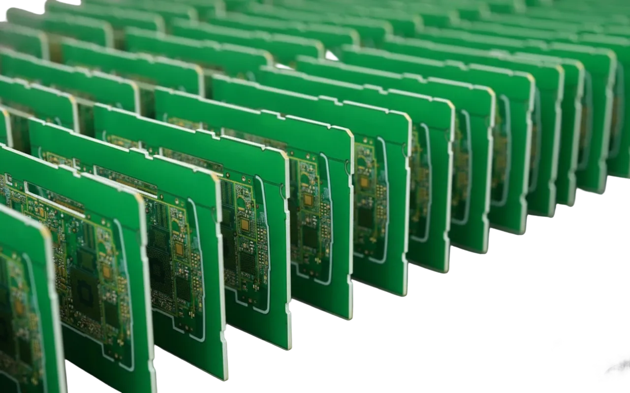
- Critical Rule: Always panelize your design. Single boards are inefficient for assembly machines and increase handling time.
- Common Pitfall: Specifying "exotic" materials with long lead times for a batch that needs to be delivered in 5 days. Stick to standard FR4 (e.g., IT-180A or S1000-2) unless RF performance dictates otherwise.
- Verification Method: Insist on Flying Probe Testing for 100% of the batch. It avoids the high NRE cost of a Bed of Nails fixture while ensuring every net is electrically verified.
- Surface Finish: Choose ENIG (Electroless Nickel Immersion Gold) over OSP. ENIG offers better shelf life and planarity for fine-pitch components, which is crucial if the batch assembly is staggered over time.
- Solder Mask: Ensure solder mask dams between pads are at least 4mil (0.1mm) to prevent solder bridging during the wave or reflow process.
Highlights
- Cost Structure: Small batch pricing is dominated by setup fees (CAM, laser plotting) rather than material costs. Optimizing panel usage is key to reducing unit price.
- Testing Strategy: Moving from visual inspection (prototypes) to automated electrical testing (small batch) is non-negotiable to prevent "dead-on-arrival" boards.
- Scalability Check: This is your final chance to catch DFM issues—like acid traps or insufficient thermal relief—before they become million-dollar problems in mass production.
- Turnaround Time: Standard lead times for small batches are typically 3-8 days, depending on layer count and complexity.
Small Batch PCB Fabrication: Definition and Scope
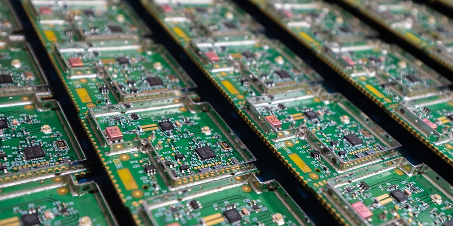
Small batch fabrication is distinct from prototyping because the manufacturing intent changes. In prototyping, the goal is functionality (does it work?). In small batch fabrication, the goal is repeatability (can we make 500 of them efficiently?).
This stage is often referred to as NPI (New Product Introduction) or Pilot Run. It involves using the same equipment that will be used for mass production—automated optical inspection (AOI), automatic pick-and-place, and reflow ovens—but with tooling strategies adapted for lower volumes. For example, instead of a permanent steel stencil, we might use a framed laser-cut stainless steel stencil. Instead of a dedicated electrical test fixture, we utilize flying probe testers that move probes rapidly to test points.
Understanding the levers you can pull during this phase is essential for controlling costs and quality.
Tech / Decision Lever → Practical Impact
| Decision Lever / Spec | Practical Impact (Yield/Cost/Reliability) |
|---|---|
| Panelization Strategy | Proper panel borders and fiducials increase assembly throughput by 30-50% and reduce handling damage. |
| Electrical Test Method | Flying Probe saves $300-$1000 in fixture costs for batches <1000 units, though it takes longer per board. |
| Via Tenting/Plugging | Fully plugging vias (IPC-4761 Type VII) prevents solder theft during assembly but adds cost. Tenting is cheaper but riskier for BGA designs. |
| Surface Finish Selection | ENIG is the gold standard for small batches due to flat pads and oxidation resistance, ensuring reliable soldering even if assembly is delayed. |
Small Batch PCB Fabrication Rules and Specifications
When moving to a small batch, adherence to standard manufacturing capabilities becomes critical to avoid yield loss. While we can manufacture tighter specs, sticking to "standard" parameters keeps costs down and yields high.
| Rule | Recommended Value | Why it matters | How to verify |
|---|---|---|---|
| Min Trace / Space | 4mil / 4mil (0.1mm) | Below this requires specialized etching control and increases risk of shorts/opens. | Run DRC (Design Rule Check) in your CAD tool. |
| Min Mechanical Drill | 0.2mm (8mil) | Smaller holes require laser drilling (HDI), significantly increasing cost. | Check drill table in Gerber files. |
| Annular Ring | 4mil (0.1mm) min | Ensures the drill hole remains within the copper pad despite mechanical tolerances. | Visual check in Gerber viewer or DFM analysis. |
| Copper Weight | 1oz (35µm) | Standard for most power/signal needs. 2oz+ requires wider spacing (etch compensation). | Specify in fabrication notes / stackup. |
| Solder Mask Dam | 4mil (0.1mm) | Prevents solder bridges between adjacent pads, especially on ICs. | Measure mask slivers in CAM software. |
| Bow & Twist | < 0.75% | Boards must be flat for automated assembly (SMT) machines to pick and place accurately. | Post-fabrication quality report. |
For more detailed capabilities regarding specific technologies, you can review our NPI and Small Batch Manufacturing page.
Small Batch PCB Fabrication Implementation Steps
Executing a small batch run requires a systematic approach to ensure the transition from design to physical board is seamless.
Implementation Process
Step-by-step execution guide
Before CAM engineering begins, we perform a deep DFM check. We look for acid traps, slivers, and unconnected nets. This is the stage to catch design errors that could ruin the entire batch.
Verify that the specified laminate (e.g., Rogers, High-TG FR4) is in stock. For impedance-controlled boards, we simulate the stackup to confirm trace widths match the target impedance.
The boards go through drilling, plating, etching, and lamination. In small batches, we use automated optical inspection (AOI) after etching inner layers to ensure no open/short circuits exist before lamination.
Every board undergoes 100% electrical testing (Flying Probe). We also perform cross-section analysis on a coupon to verify plating thickness and hole wall integrity.
Small Batch PCB Fabrication Troubleshooting
Even with careful planning, issues can arise. Here are common problems in small batch runs and how to fix them.
1. Warpage (Bow and Twist)
- Symptom: The PCB is not flat, causing placement errors during SMT assembly or reflow issues.
- Cause: Unbalanced copper distribution (e.g., a solid ground plane on layer 2 but sparse routing on layer 3) creates uneven stress during thermal cycles.
- Fix: Use copper thieving (hatching) in open areas to balance the copper density across the stackup. Ensure the stackup is symmetrical around the center core.
2. Solderability Issues
- Symptom: Solder does not wet properly to the pads, leading to cold joints.
- Cause: Oxidation of the surface finish (common with OSP if stored improperly) or insufficient plating thickness.
- Fix: For small batches, switch to ENIG or Immersion Silver. If using OSP, ensure boards are vacuum-sealed and baked before assembly if moisture indicators are pink.
3. Component Misalignment
- Symptom: Parts are rotated or shifted off pads.
- Cause: Lack of fiducials on the panel rails or the board itself.
- Fix: Always include at least three global fiducials on the panel rails and local fiducials for fine-pitch components (BGA, QFN).
For more on ensuring your design is ready for manufacturing, consult our DFM Guidelines.
Supplier Qualification Checklist: How to Vet Your Fab
Not all manufacturers are optimized for small batch work. Some are prototype-only shops that lack rigorous controls, while others are mass-production giants that won't prioritize a 200-unit order. Use this checklist to vet your partner:
- Do you perform 100% electrical testing on small batches? (Answer should be YES, usually via Flying Probe).
- What is your standard tolerance for impedance control? (Standard is ±10%, advanced is ±5%).
- Do you offer in-house assembly (PCBA) for small batches? (Integrated services reduce logistics risks).
- Can you provide a cross-section report (microsection) for the batch? (Essential for verifying via quality and plating thickness).
- What is your policy on X-Outs (defective boards in a panel)? (Ensure you agree on whether X-outs are allowed; usually <5% is standard).
- Do you review files for DFM before starting? (Automated checks are good, but human engineering review is better).
- What are your storage conditions for moisture-sensitive materials? (Critical for flex and rigid-flex boards).
Glossary
NPI (New Product Introduction): The process of taking a product from design to a final manufacturing form. Small batch fabrication is a key subset of NPI.
Flying Probe Test: A fixtureless method of electrical testing where robotic probes move to test points. It is slower than a bed-of-nails test but requires no tooling cost, making it ideal for small batches.
Panelization: The practice of arranging multiple PCB instances on a larger "panel" (array) to facilitate efficient assembly. It includes tooling rails, fiducials, and tooling holes.
Fiducial Marker: A copper feature (usually a circle) used by vision systems in assembly machines to orient the PCB and calculate precise component placement coordinates.
X-Out: A defective individual PCB within a larger panel array. Manufacturers usually mark these with a permanent marker so the assembly machine skips them.
6 Essential Rules for Small Batch PCB Fabrication (Cheat Sheet)
| Rule / Guideline | Why It Matters (Physics/Cost) | Target Value / Action |
|---|---|---|
| Panelize Designs | Assembly machines need rails to hold the board. Single units slow down production. | 2x3 or 3x4 Array with 5-10mm rails |
| Use Standard Stackups | Custom stackups require ordering specific prepreg/core, adding days to lead time. | JLC04161H-3313 or similar standard |
| Define Impedance | High-speed signals reflect without matching. Fab must adjust trace width. | 50Ω / 90Ω / 100Ω (±10%) |
| 100% Electrical Test | Visual inspection misses internal shorts/opens. Bad boards = wasted components. | Flying Probe (Mandatory) |
| Add Fiducials | Cameras need reference points for accurate placement of fine-pitch parts. | 3 Global + Local for BGAs |
| Solder Mask Dams | Prevents solder bridging on IC pins. | Min 4mil (0.1mm) |
FAQ
Q: What is the typical lead time for a small batch (e.g., 200 units)?
A: Standard lead time is usually 5-8 working days for fabrication. If you include assembly, add another 1-2 weeks for component procurement and mounting. Expedited services (24-48 hours) are available but come with a premium.
Q: Can I combine multiple different designs into one small batch order?
A: Yes, this is called a "multi-part panel" or "family panel." However, it can complicate separation (depanelization) and assembly if the quantities for each design are not identical. It is often better to run them as separate line items for clarity.
Q: Is hard gold plating necessary for small batches?
A: Only if the PCB has edge connectors that will be inserted/removed repeatedly (like a PCIe card). For standard component soldering, ENIG is superior and more cost-effective.
Q: How do I handle component sourcing for small batches?
A: You can supply the parts (Consigned) or have the manufacturer source them (Turnkey). For small batches, Turnkey Assembly is often preferred to save you the logistics headache of managing 50 different BOM lines.
Q: What happens if I find a design error after the batch has started?
A: Once the CAM engineering is approved and films/tools are generated, changes are difficult and costly. If the boards are already etched, they must be scrapped. This highlights the importance of the initial DFM review.
Q: Do you support rigid-flex PCBs for small batch runs?
A: Yes, we specialize in complex technologies including Rigid-Flex PCBs. Note that lead times for rigid-flex are typically longer (10-15 days) due to the complex lamination and coverlay processes involved.
Request a Quote / DFM Review for Small Batch PCB Fabrication
To get an accurate quote and DFM review for your small batch run, please prepare the following:
- Gerber Files: RS-274X format (include all copper layers, drill files, solder mask, and silkscreen).
- Fabrication Drawing: Specify material (e.g., FR4 TG150), thickness (e.g., 1.6mm), copper weight, and surface finish.
- Stackup Details: If impedance control is required, specify the target impedance and reference layers.
- Quantity: State the exact number of pieces or panels required.
- Assembly Info (if applicable): BOM (Bill of Materials) and Pick & Place (XY) file.
Conclusion
Small batch pcb fabrication is the bridge between a working idea and a market-ready product. By adhering to standard design rules, utilizing proper panelization, and insisting on rigorous testing like flying probe and AOI, you can ensure your pilot run is a success. At APTPCB, we treat every small batch with the same rigor as mass production, ensuring your transition to volume manufacturing is smooth and risk-free.
Signed, The Engineering Team at APTPCB