Software Defined Radar (SDRadar) represents a shift from fixed hardware architectures to flexible, programmable systems where waveform generation and signal processing are handled by software. For PCB designers and engineers, this transition introduces complex challenges in mixed-signal integrity, thermal management, and high-frequency material selection. Unlike traditional radar, where the hardware defines the function, SDRadar requires a physical platform capable of supporting varying waveforms, frequencies (such as 24GHz, 77GHz, and 79GHz), and processing loads without hardware redesigns.
This guide provides the technical specifications, implementation steps, and troubleshooting protocols necessary to manufacture reliable Software Defined Radar hardware.
Quick Answer (30 seconds)
Successful Software Defined Radar implementation relies on minimizing signal loss while maximizing digital processing density.
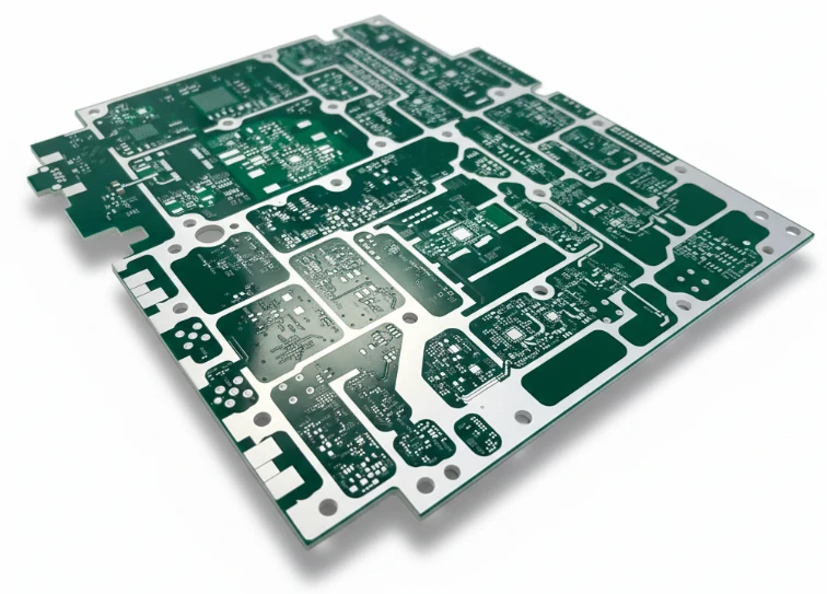
- Material Selection: Use hybrid stackups combining high-frequency laminates (e.g., Rogers RO3003/RO4835) for RF layers and high-Tg FR4 for digital control layers to balance performance and cost.
- Impedance Control: Maintain strict 50Ω (single-ended) and 100Ω (differential) impedance on RF lines; tolerances must be within ±5% to prevent signal reflection at millimeter-wave frequencies.
- Thermal Management: SDRadar relies heavily on FPGAs or high-end DSPs; implement copper coin technology or dense thermal via arrays to dissipate heat from digital components without affecting RF stability.
- Surface Finish: Utilize Electroless Nickel Immersion Gold (ENIG) or Immersion Silver to ensure a flat surface for fine-pitch components and minimize insertion loss at high frequencies.
- Layer Registration: Ensure layer-to-layer registration accuracy is within ±3 mils to maintain antenna array alignment and beamforming precision.
- Validation: Verify Dielectric Constant (Dk) stability across the operating temperature range (-40°C to +85°C) to prevent frequency drift in ADAS applications.
When Software Defined Radar applies (and when it doesn’t)
Understanding the operational context ensures that the complexity of an SDRadar architecture is justified by the application requirements.
When Software Defined Radar is the right choice:
- Multi-Mode Operations: When the system must switch between long-range detection and short-range wide-angle imaging (e.g., 4D Radar PCB applications) dynamically.
- Rapid Prototyping & Research: When algorithms and waveforms are still in development, allowing engineers to update functionality via firmware without respining the PCB.
- Complex Interference Environments: In scenarios requiring cognitive radar capabilities to detect and avoid jamming or interference from other ADAS systems.
- High-Resolution Imaging: When advanced beamforming and MIMO (Multiple Input Multiple Output) techniques are required to generate point clouds similar to LiDAR.
- Regulatory Compliance: When a single hardware platform must adapt to different regional frequency allocations (e.g., switching between 76-77GHz and 77-81GHz).
When to stick with traditional hardware radar:
- Ultra-Low Cost Consumer Electronics: Simple motion sensors or automatic door openers where the cost of FPGAs and high-grade PCBs is prohibitive.
- Extreme Power Constraints: Battery-operated IoT devices where the power consumption of high-speed ADCs and processors in SDRadar is unsustainable.
- Fixed, Single-Function Applications: Systems that only require basic distance measurement with no need for waveform agility or classification.
- Legacy Industrial Systems: Environments with established, certified hardware loops where introducing software-defined variability creates unnecessary validation risks.
Rules & specifications
The physical realization of Software Defined Radar demands adherence to strict manufacturing rules. Deviations in PCB fabrication can render sophisticated software algorithms useless due to hardware-induced noise or phase errors.
| Rule | Recommended Value/Range | Why it matters | How to verify | If ignored |
|---|---|---|---|---|
| Dielectric Constant (Dk) Tolerance | ±0.05 or better | Direct impact on phase velocity and antenna resonance frequency. | IPC-TM-650 2.5.5.5 test method on test coupons. | Frequency shift; beam steering errors in phased arrays. |
| Copper Surface Roughness | VLP (Very Low Profile) or HVLP (< 1 µm) | Skin effect at 77GHz makes current flow on the surface; roughness increases resistance and loss. | SEM (Scanning Electron Microscope) analysis of foil. | High insertion loss; reduced radar range and sensitivity. |
| Trace Width Accuracy | ±10% or ±0.5 mil (whichever is tighter) | Determines characteristic impedance; critical for matching networks. | Cross-section analysis (microsectioning) after etching. | Impedance mismatch; signal reflections; standing waves. |
| Solder Mask Clearance | 2-3 mils (or defined by DFM) | Solder mask over RF lines adds variable Dk, altering impedance. | Automated Optical Inspection (AOI). | Unpredictable impedance shifts; increased signal loss. |
| Via Stitching Pitch | < λ/20 at operating frequency | Prevents substrate integrated waveguide (SIW) leakage and creates a Faraday cage. | DRC (Design Rule Check) in CAD; visual inspection. | RF leakage; crosstalk between transmit and receive channels. |
| Layer-to-Layer Registration | < 3 mils | Critical for coupling structures and vertical transitions (vias) in multilayer boards. | X-ray inspection of the laminated stackup. | Misalignment of antenna feeds; signal attenuation; open circuits. |
| Plating Thickness (ENIG) | Ni: 3-6 µm, Au: 0.05-0.15 µm | Affects skin depth conductivity and solder joint reliability. | X-ray Fluorescence (XRF) measurement. | "Black pad" syndrome (brittle joints) or increased RF loss. |
| Thermal Via Density | 0.3mm - 0.5mm pitch under pads | High-performance FPGAs generate significant heat; efficient transfer to ground planes is needed. | Thermal simulation; post-assembly thermal imaging. | Processor throttling; system shutdown; component failure. |
| Moisture Absorption | < 0.1% | Water (Dk ~80) absorbed into the substrate changes the effective Dk of the material. | Pressure Cooker Test (PCT) or weight gain analysis. | Performance drift in humid environments; delamination during reflow. |
| CTE (Z-axis) | < 50 ppm/°C | Prevents barrel cracks in plated through-holes during thermal cycling. | TMA (Thermomechanical Analysis). | Via failure; intermittent open circuits in harsh automotive conditions. |
| Etch Factor | ≥ 3:1 (Trapezoidal shape control) | Rectangular traces are ideal; trapezoidal shapes change effective width and impedance. | Microsection analysis. | Impedance discontinuities; model-to-hardware mismatch. |
| Blind/Buried Via Aspect Ratio | 0.8:1 to 1:1 | Ensures reliable plating inside the via hole. | Microsection analysis. | Incomplete plating; voids in vias; electrical failure. |
Implementation steps

Building a Software Defined Radar system requires a disciplined workflow that integrates RF physics with digital logic design. APTPCB (APTPCB PCB Factory) recommends the following step-by-step approach to ensure manufacturability and performance.
Step 1: System Architecture & Frequency Definition Define the operating frequency bands (e.g., 24GHz for blind spot, 77GHz for long-range). Determine the number of TX/RX channels required for the desired angular resolution.
- Key Parameter: Bandwidth requirements (e.g., 4GHz sweep for high resolution).
- Acceptance Check: Block diagram confirmed with component availability.
Step 2: Material Selection & Stackup Design Select materials based on frequency and cost. For 77GHz, materials like Rogers RO3003 are standard for RF layers. Design a hybrid stackup using FR4 for digital/power layers to reduce cost.
- Key Parameter: Dk stability vs. Frequency and Temperature.
- Acceptance Check: Stackup simulation confirms impedance targets (50Ω/100Ω) are achievable with manufacturable trace widths.
- Resource: Consult RF Rogers material properties for specific Dk values.
Step 3: RF Layout & Antenna Design Route RF transmission lines first. Keep lines as short as possible. Design the antenna array (patch, slot, or comb) directly on the top layer. Ensure ground cutouts are precise.
- Key Parameter: Isolation between TX and RX (> 40dB).
- Acceptance Check: EM simulation (HFSS/ADS) shows acceptable return loss (S11 < -10dB) and isolation.
Step 4: Digital & Power Layout Place the FPGA/DSP and ADCs close to the RF front end but separated by shielding or guard rings. Route high-speed digital interfaces (DDR, PCIe) with length matching.
- Key Parameter: Power Distribution Network (PDN) impedance.
- Acceptance Check: Signal Integrity (SI) simulation passes eye diagram requirements.
Step 5: Thermal Management Strategy Implement thermal vias under the main processors and RF MMICs. If power density is high, consider embedded copper coins or metal-backed PCBs.
- Key Parameter: Junction temperature (Tj) < 125°C (or component max).
- Acceptance Check: Thermal simulation confirms heat dissipation paths are sufficient.
Step 6: Design for Manufacturing (DFM) Review Check minimum trace/space, via aspect ratios, and solder mask clearances against the manufacturer's capabilities.
- Key Parameter: Min trace/space (e.g., 3/3 mil for standard, tighter for HDI).
- Acceptance Check: DFM Guidelines review passes with zero critical errors.
Step 7: Fabrication & Etching Fabricate the PCB with strict control over etching to maintain trace width accuracy. Use controlled depth drilling for blind vias.
- Key Parameter: Etch tolerance (±10%).
- Acceptance Check: Impedance test coupons measured via TDR (Time Domain Reflectometry).
Step 8: Assembly & Reflow Assemble components using a profile compatible with the hybrid material stackup. Ensure precise placement of BGA components.
- Key Parameter: Reflow peak temperature and time above liquidus.
- Acceptance Check: X-ray inspection of BGA solder joints (voiding < 25%).
Step 9: Functional Testing & Calibration Power up the board and load the firmware. Perform initial calibration to correct for phase mismatches in the antenna array.
- Key Parameter: Noise floor and dynamic range.
- Acceptance Check: Radar detects a corner reflector at a known distance with correct RCS (Radar Cross Section).
Failure modes & troubleshooting
Even with robust design, issues can arise during the integration of Software Defined Radar. This section outlines common failure modes and their resolutions.
1. Symptom: Ghost Targets or False Positives
- Causes: Signal reflections due to impedance mismatch; multipath interference from radome or housing; coupling between TX and RX lines.
- Checks: Verify TDR measurements for impedance discontinuities. Check isolation between channels. Inspect radome material and distance.
- Fix: Tune matching networks. Add microwave absorbing material to the housing. Improve shielding between sections.
- Prevention: Strict adherence to impedance control rules and proper guard ring implementation.
2. Symptom: Reduced Detection Range
- Causes: High insertion loss in the PCB material; excessive surface roughness; moisture absorption; poor solder joints on the MMIC.
- Checks: Measure insertion loss on test coupons. Inspect surface finish quality. Check for "black pad" on ENIG.
- Fix: Switch to lower loss material (lower Df). Use HVLP copper. Re-flow or re-ball BGA if joints are suspect.
- Prevention: Use Impedance Calculator to verify loss budget during design.
3. Symptom: Frequency Drift over Temperature
- Causes: High Thermal Coefficient of Dielectric Constant (TCDk) of the substrate material; oscillator instability.
- Checks: Test system in a thermal chamber (-40°C to +85°C). Monitor LO (Local Oscillator) frequency.
- Fix: Implement software compensation algorithms. Change to a material with TCDk < 50 ppm/°C.
- Prevention: Select materials specifically designed for automotive radar environments (e.g., Rogers RO3003).
4. Symptom: Digital Noise Coupling into RF Spectrum
- Causes: Poor grounding; shared power planes between analog and digital; lack of via stitching.
- Checks: Spectrum analysis looking for spurs at clock harmonics. Review stackup for return path breaks.
- Fix: Add shielding cans. Improve decoupling capacitor placement. Separate analog and digital grounds (or use a solid unified ground with careful placement).
- Prevention: Proper floorplanning and partitioning of the PCB layout.
5. Symptom: Delamination during Assembly
- Causes: Mismatched CTE between hybrid materials (FR4 vs. PTFE); moisture trapped in the board.
- Checks: Visual inspection for blistering. Cross-section analysis.
- Fix: Bake boards before assembly to remove moisture. Adjust reflow profile ramp rates.
- Prevention: Use high-Tg FR4 materials compatible with the lamination cycle of the RF material.
6. Symptom: Phase Errors in Beamforming
- Causes: Trace length mismatch; variations in Dk across the panel; etching variations.
- Checks: Measure phase delay on VNA. Check trace width consistency.
- Fix: Software calibration (phase shifting).
- Prevention: Use "spread glass" or non-woven glass styles to minimize local Dk variations (Fiber Weave Effect).
Design decisions
Connecting the failure modes to proactive engineering choices is vital. In Software Defined Radar, the hardware must be "transparent" to the software—meaning it should not introduce unknown variables.
Centralized vs. Edge Processing Deciding where the signal processing happens impacts the PCB layout significantly.
- Edge Processing: The radar module contains the FPGA/DSP. This requires a complex, high-layer-count HDI PCB with advanced thermal management but reduces data bandwidth to the central computer.
- Centralized Processing: The radar module sends raw data (via MIPI CSI-2 or LVDS) to a central ECU. The radar PCB is simpler (mostly RF + Transceiver), but the data link requires high-speed connector and cable integrity.
Antenna Array Structure (MIMO) To achieve 4D imaging (Range, Doppler, Azimuth, Elevation), designers use MIMO arrays.
- Virtual Array: Using sparse physical arrays to create a larger virtual aperture. This requires precise spacing (typically λ/2).
- Decision: The PCB manufacturing tolerance for feature location becomes critical here. A 50-micron error in antenna placement can degrade the side-lobe suppression levels.
Material Cost vs. Performance Trade-off
- Pure PTFE: Best performance, highest cost, difficult to process (soft).
- Ceramic-filled Hydrocarbon: Good balance, easier to process, stable Dk.
- Hybrid: The industry standard for cost-effective volume production. The decision involves selecting a prepreg that bonds well with both the RF core and the FR4 core without delamination.
FAQ
Q1: What is the main difference between traditional radar and Software Defined Radar hardware? Traditional radar often uses fixed hardware blocks for signal processing. SDRadar relies on high-speed ADCs and FPGAs/DSPs to process waveforms digitally, requiring PCBs that support both extremely high frequencies (RF) and high-speed digital data simultaneously.
Q2: Which PCB materials are best for 77GHz Software Defined Radar? Materials with extremely low Dielectric Constant (Dk) and Dissipation Factor (Df) are required. Common choices include Rogers RO3003, RO4835, or Taconic TLY-5. For cost efficiency, these are often used in a hybrid stackup with high-Tg FR4.
Q3: How does APTPCB handle the manufacturing of hybrid stackups? APTPCB uses specialized lamination cycles to bond dissimilar materials (e.g., PTFE and FR4) ensuring adhesion without damaging the RF layer. We also manage the different scaling factors of materials to ensure registration accuracy.
Q4: Why is surface finish critical for 77GHz Radar PCBs? At 77GHz, the "skin depth" of the signal is very shallow. Rough surfaces or finishes with high resistance (like HASL) cause significant signal loss. ENIG or Immersion Silver provides a flat, conductive surface ideal for these frequencies.
Q5: Can I use standard FR4 for 24GHz Radar applications? Standard FR4 has a high Df and inconsistent Dk at 24GHz, leading to high loss and poor performance. While some high-performance FR4 variants exist, specialized high-frequency laminates are strongly recommended for reliability.
Q6: What is the lead time for manufacturing a Software Defined Radar PCB? Lead times depend on material availability. Standard materials are stocked, but specialized RF laminates may have lead times of 2-4 weeks. Once materials are secured, fabrication typically takes 5-10 days depending on complexity (HDI, blind vias).
Q7: How do you verify impedance control at millimeter-wave frequencies? We use TDR (Time Domain Reflectometry) on test coupons designed to match the actual traces on the board. For 77GHz, we also rely on strict cross-section analysis to verify trace geometry and dielectric thickness.
Q8: What are the specific DFM challenges for 4D Radar PCBs? 4D Radar requires dense antenna arrays and high channel counts (MIMO). The main challenges are fine-pitch BGA routing (0.4mm or less), via-in-pad technology, and maintaining strict flatness (coplanarity) for large sensor chips.
Q9: How does the "Fiber Weave Effect" impact Radar PCBs? If a narrow RF trace runs directly over a glass bundle in the laminate, it sees a different Dk than if it runs over the resin gap. This causes phase skew. We recommend using "spread glass" or rotating the design 10 degrees to average out these effects.
Q10: Is it necessary to use blind and buried vias? For compact SDRadar modules, yes. Blind and buried vias allow for the isolation of digital and RF grounds and enable the routing of high-density interconnects without penetrating the RF layers unnecessarily.
Q11: How does APTPCB ensure the thermal reliability of the PCB? We implement copper coin embedding, heavy copper layers, and optimized thermal via arrays. We also perform thermal stress testing (IST or solder float) to ensure via reliability under thermal cycling.
Q12: What data do I need to provide for a quote? Please provide Gerber files, the BOM (if assembly is needed), and a detailed fabrication drawing specifying the material type (or Dk/Df requirements), stackup, impedance requirements, and surface finish.
Related pages & tools
To further assist in your design process, utilize these APTPCB resources:
- PCB Manufacturing Services: Explore our capabilities for HDI and RF boards.
Glossary (key terms)
| Term | Definition | Context in SDRadar |
|---|---|---|
| FMCW | Frequency Modulated Continuous Wave | The most common waveform used in automotive radar for measuring range and velocity. |
| MIMO | Multiple Input Multiple Output | Using multiple TX and RX antennas to create a larger virtual aperture for higher angular resolution. |
| Dk (εr) | Dielectric Constant | A measure of a material's ability to store electrical energy; determines signal speed and impedance. |
| Df (tan δ) | Dissipation Factor | A measure of signal loss (energy dissipated as heat) in the dielectric material. |
| Skin Effect | Skin Effect | The tendency of high-frequency current to flow only on the outer surface of the conductor. |
| Phase Noise | Phase Noise | Random fluctuations in the phase of a waveform; critical for detecting slow-moving targets. |
| Beamforming | Beamforming | A signal processing technique used to direct radio waves in a specific direction using antenna arrays. |
| Chirp | Chirp | A signal in which the frequency increases (up-chirp) or decreases (down-chirp) with time. |
| Hybrid Stackup | Hybrid Stackup | A PCB layer buildup using different materials (e.g., PTFE and FR4) to optimize cost and performance. |
| SIW | Substrate Integrated Waveguide | A waveguide structure synthesized on a PCB using rows of vias and metal planes. |
| RCS | Radar Cross Section | A measure of how detectable an object is by radar. |
| HDI | High Density Interconnect | PCB technology using microvias, blind/buried vias, and fine lines to increase component density. |
Conclusion
Software Defined Radar is transforming the landscape of sensing technology, moving from rigid hardware to adaptable, intelligent systems. However, the flexibility of software relies entirely on the precision of the underlying hardware. A minor deviation in PCB material properties, a slight etching error, or poor thermal management can compromise the sophisticated algorithms driving the system.
For engineers developing 77GHz, 79GHz, or 4D imaging radar, the choice of manufacturing partner is as critical as the code itself. APTPCB combines advanced material handling, precise etching capabilities, and rigorous quality control to deliver PCBs that meet the demanding specifications of modern radar systems.
Whether you are in the prototyping phase or ready for mass production, ensure your hardware foundation is solid.
Ready to build your Software Defined Radar platform? Request a Quote today or contact our engineering team to discuss your stackup and DFM requirements.