
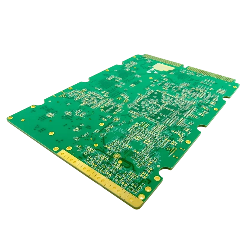
What should you consider before choosing a soil moisture wireless PCB?
A soil moisture wireless PCB must solve two problems at the same time: accurate environmental measurement and reliable wireless communication in a harsh outdoor environment.
Agricultural sensor electronics operate differently from consumer IoT devices. A field-installed node may experience continuous humidity, fertilizer exposure, temperature cycling, soil chemicals, condensation, and years of battery operation. A design that works on a laboratory bench can still fail after months underground.
A production-ready board typically combines:
- Capacitive soil moisture sensing
- Low-power MCU operation
- Wireless communication such as LoRaWAN, NB-IoT, Zigbee, or BLE
- Battery management optimized for multi-year deployment
- Environmental protection through conformal coating or potting
- Controlled RF performance after final enclosure assembly
This guide helps hardware engineers, product managers, and procurement teams evaluate PCB suppliers and define requirements before requesting quotes.
When is a wireless soil moisture PCB the right architecture?
A custom wireless PCB is a strong fit when the product requires:
| Requirement | Recommended architecture |
|---|---|
| Large agricultural fields | Battery-powered wireless nodes using LoRaWAN or cellular IoT |
| Frequent irrigation decisions | Sensor nodes with scheduled measurements and cloud connectivity |
| Thousands of deployed units | Custom PCB with optimized BOM and automated assembly |
| Long outdoor lifetime | Protected PCB assembly with validated materials and coatings |
A different architecture may be better when the installation has short cable distances, requires extremely deep sensing, or only needs temporary testing. For deep soil measurements, keeping the antenna electronics above ground while extending a sensor probe can provide better communication performance.
Which PCB specifications matter most for soil moisture sensors?
The most important specifications are environmental protection, RF stability, power efficiency, and manufacturing consistency.
Soil moisture wireless PCB selection matrix
| Design decision | Option A | Option B | Engineering choice |
|---|---|---|---|
| Wireless frequency | 2.4 GHz BLE/Zigbee | Sub-GHz LoRa/915 MHz | Sub-GHz generally provides better outdoor range and soil-adjacent performance |
| PCB stackup | 2-layer FR4 | 4-layer controlled impedance | Choose 4-layer for improved RF routing and noise control |
| Protection | Conformal coating | Full potting | Coating improves repairability; potting maximizes environmental protection |
| Sensor method | Resistive probe | Capacitive sensing | Capacitive sensing provides better corrosion resistance |
| Antenna | PCB trace antenna | External antenna connector | PCB antenna reduces assembly complexity; external antenna improves flexibility |
| Surface finish | HASL | ENIG | ENIG provides better flatness and corrosion resistance for fine-pitch RF components |
What materials should be specified for a soil moisture wireless PCB?
Clear material specifications prevent suppliers from selecting unsuitable standard options.
PCB substrate and stackup
Specify:
- High-Tg FR4 with Tg above 170°C for demanding thermal environments
- Controlled impedance for RF antenna traces
- Low moisture absorption laminate when long-term insulation performance is critical
- Four-layer Ground-Signal-Signal-Ground stackup when RF performance and noise isolation are priorities
For specialized high-frequency applications, RF laminates such as Rogers materials may be considered. Standard FR4 is commonly suitable for sub-GHz LoRa designs.
Surface finish and solder mask
Recommended specifications:
- ENIG surface finish for RF modules and fine-pitch components
- High-quality LPI solder mask
- Filled or plugged vias where potting compound migration could create problems
- Controlled solder mask coverage around sensing areas
Copper and electrical requirements
Typical requirements include:
- Minimum 1 oz copper for standard sensor electronics
- 2 oz copper when powering higher-current loads such as valves or actuators
- 50Ω antenna impedance with documented control
- Low leakage current design for battery-powered deployments
Agricultural sensor products often depend on years of unattended operation, making PCB insulation quality as important as circuit design.
What causes soil moisture wireless PCB failures?
Field failures usually result from environmental interactions rather than schematic errors.
Soil sensor PCB failure-mode table
| Failure mode | Root cause | Detection method | Prevention |
|---|---|---|---|
| Electrochemical migration | Moisture, contamination, and voltage create conductive paths | Humidity testing and field failure analysis | Ionic cleanliness testing and protective coating |
| RF range reduction | Potting material changes antenna characteristics | Compare RF performance before and after enclosure sealing | Tune antenna with final enclosure materials |
| Battery drain | PCB leakage paths or poor sleep-current design | Current profiling during sleep and transmit cycles | Use low-leakage materials and validate standby current |
| Via cracking | Thermal expansion mismatch during cycling | Thermal shock and electrical continuity testing | Use reliable plating processes and robust via structures |
| Sensor drift | PCB moisture absorption changes capacitance | Long-term calibration testing | Use stable sensor geometry and sealed sensing regions |
| Component cracking | Mechanical stress from potting shrinkage | X-ray inspection and failure analysis | Select compatible potting materials |
How should a soil moisture wireless PCB be validated?
Production qualification should simulate the actual agricultural environment.
Environmental and electrical validation plan
| Test | Purpose | Typical acceptance target |
|---|---|---|
| Surface Insulation Resistance (SIR) | Verify cleanliness and leakage resistance | Resistance remains above 100 MΩ after humidity exposure |
| Thermal cycling | Validate vias and solder joints | No electrical opens after repeated cycling |
| Salt spray testing | Simulate corrosive environments | No conductor corrosion or coating breakdown |
| RF testing after potting | Confirm wireless performance | Frequency shift and range degradation remain within design limits |
| Water immersion | Validate enclosure protection | No ingress during IP-rated testing |
| Battery profiling | Confirm lifetime calculations | Measured current matches design model within expected tolerance |
| Soil calibration testing | Validate measurement accuracy | Repeatable readings across representative soil types |
| Vibration testing | Validate transport and installation durability | No loose components or intermittent connections |
How do you choose a soil moisture wireless PCB supplier?
The supplier should demonstrate both PCB manufacturing capability and experience with outdoor electronics.
RFQ supplier checklist
Design package requirements
- Gerber files and drill files
- PCB stackup requirements
- Controlled impedance requirements
- BOM with approved components
- Coating or potting specifications
- Test requirements including RF and functional testing
Manufacturing capability
- Automated optical inspection after SMT
- X-ray inspection for wireless modules and hidden joints
- Impedance testing capability
- Ionic contamination testing
- Conformal coating process control
- Traceability for PCB materials and component batches
Quality system
- ISO 9001 quality management system
- Certificate of Conformance with shipments
- Engineering change notification process
- Non-conforming material review process
- Component substitution approval workflow
Which soil moisture wireless PCB trade-offs should engineers make?
Integrated PCB antenna vs external antenna
A PCB trace antenna reduces BOM cost and simplifies assembly. An external antenna connector provides more flexibility when enclosure placement or installation conditions reduce RF performance.
Conformal coating vs full potting
Conformal coating provides environmental protection while maintaining serviceability. Full potting offers maximum moisture resistance and mechanical protection but makes repair difficult.
PCB-integrated sensor vs external probe
A PCB sensing element provides compact integration and lower assembly cost. External probes provide easier replacement and can simplify calibration across different soil conditions.
Two-layer vs four-layer PCB
A two-layer design can reduce cost for simple circuits. Four-layer boards provide better grounding, RF control, and noise management for advanced wireless sensor systems.
Frequently asked questions about soil moisture wireless PCB design
How far can a wireless soil moisture PCB transmit?
Range depends on frequency, antenna design, installation depth, soil moisture, and surrounding obstacles. Sub-GHz technologies such as LoRa typically provide better range characteristics than 2.4 GHz systems in outdoor agricultural deployments.
Can a soil moisture PCB be buried underground?
The sensing portion can be buried, but wireless performance decreases when antennas are surrounded by wet soil. Many designs place the radio section near the surface while extending the sensor element into the soil.
Is capacitive sensing better than resistive sensing?
Capacitive sensing is commonly preferred for long-life agricultural products because it does not require current flow through exposed electrodes, reducing corrosion problems.
Does a soil sensor PCB need UL certification?
Requirements depend on product category, market, voltage levels, and regulatory environment. Battery-powered low-voltage sensors may not require the same certifications as industrial equipment, while higher-voltage agricultural systems may require additional compliance considerations.
Can standard FR4 support LoRa soil moisture sensors?
Yes. Standard FR4 is commonly used for sub-GHz wireless designs. RF-specific materials become more relevant for higher-frequency applications with tighter loss requirements.
Related pages & tools
- Industrial Control PCB: Explore how we handle high-reliability boards for industrial and agricultural automation.
- High Frequency PCB: Understand the material and process requirements for ensuring your wireless signal stays strong.
- PCB Conformal Coating: Learn about the protective layers that are essential for soil-contact electronics.
- Rigid-Flex PCB: See how rigid-flex technology can help fit sensors into compact, waterproof housings.
- Quote Request: Ready to move forward? Get a comprehensive quote that includes DFM review.
Request a quote
Ready to validate your soil moisture wireless PCB design? Submit your Gerber files, BOM, enclosure requirements, coating specifications, and testing requirements for a manufacturing review.
Conclusion
A reliable soil moisture wireless PCB requires more than wireless connectivity and a moisture sensor. Long-life agricultural deployments depend on material selection, RF validation, environmental testing, and supplier process control.
By defining the right PCB specifications before production, validating the design against real field conditions, and selecting a manufacturing partner with reliability experience, engineering teams can reduce deployment failures and scale precision agriculture products with confidence.