Solar PCB manufacturing demands specialized capabilities addressing unique challenges of photovoltaic electronics—wide input voltage ranges, high-efficiency power conversion, outdoor environmental exposure, and 25+ year operational lifetimes matching solar panel warranties. Unlike consumer electronics with 3-5 year lifecycles, solar electronics require enhanced reliability, temperature cycling resistance, and moisture protection operating continuously in harsh outdoor conditions from desert heat to arctic cold.
At APTPCB, we manufacture solar PCBs with enhanced reliability specifications supporting photovoltaic inverters, charge controllers, monitoring systems, and power optimizers. Our advanced manufacturing processes implement material selections, surface finishes, and quality controls ensuring solar electronics achieve multi-decade operational lifetimes.
Managing Wide Voltage Ranges in Solar PCB Design
Solar electronics handle input voltages spanning 12VDC battery systems through 1000VDC+ grid-tie inverters with transient overvoltages from lightning or switching events. PCB designs must provide adequate creepage, clearance, and isolation preventing arcing or tracking failures while maintaining compact dimensions for cost-effective production.
At APTPCB, our solar PCB manufacturing implements design rules and process controls ensuring electrical safety and long-term reliability.
Key High-Voltage Design Requirements
- Enhanced Creepage and Clearance: PCB layout rules maintaining minimum spacing per IEC 62109 and UL 1741 standards preventing arc-over between high-voltage traces and components.
- Isolation Barrier Implementation: Multilayer PCB stackups with dedicated isolation layers and controlled via placement achieving reinforced isolation for safety-critical applications.
- High-Voltage Material Selection: Using high-Tg FR4 or polyimide laminates with CTI ratings >400V preventing carbon tracking in high-humidity outdoor environments.
- Soldermask Coverage: Enhanced soldermask thickness and coverage protecting copper traces from environmental exposure and maintaining insulation resistance over decades.
- Partial Discharge Testing: Manufacturing process validation through corona and partial discharge testing ensuring designs remain stable under continuous high-voltage stress.
- Surface Contamination Control: Stringent cleaning processes removing ionic residues that could compromise insulation resistance in humid conditions.
Long-Term Electrical Reliability
By implementing IPC Class 3 manufacturing standards with solar-specific enhancements, APTPCB delivers PCBs maintaining insulation resistance >100MΩ after extended humidity exposure and temperature cycling. Our PCB quality processes ensure solar electronics achieve the 25-year operational lifetimes expected in photovoltaic installations.
Implementing Thermal Management for Outdoor Solar Electronics
Solar inverters and power electronics experience extreme thermal cycling—daytime operation at full power in direct sunlight followed by nighttime cooling, with ambient temperatures ranging from -40°C to +85°C depending on geographic location. Inadequate thermal design causes premature failure, degraded efficiency, or safety shutdown reducing system energy production.
APTPCB employs advanced thermal management strategies ensuring solar electronics maintain performance across environmental extremes.
Key Thermal Design Techniques
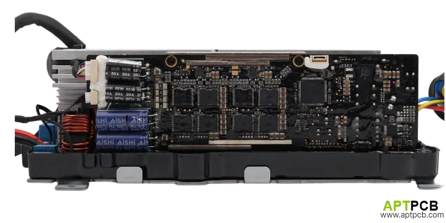
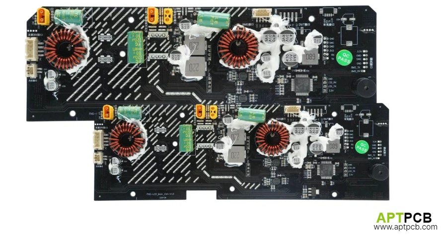
- Heavy Copper Power Distribution: Utilizing heavy copper PCB with 3-6oz copper layers spreading heat from power semiconductors while handling high DC currents without excessive voltage drop.
- Metal Core PCB Integration: Implementing metal core technology for inverter power stages achieving superior thermal conductivity and reducing junction temperatures in compact enclosures.
- Thermal Via Arrays: Dense thermal via placement beneath power components conducting heat through PCB to external heat sinks or chassis mounting surfaces.
- Material Thermal Stability: Selecting high-Tg PCB laminates maintaining dimensional stability and electrical performance during repetitive thermal cycling.
- Copper Weight Optimization: Balancing copper thickness for current capacity and thermal spreading against cost and manufacturing constraints.
- Thermal Simulation Validation: Pre-production thermal modeling identifying hot spots and optimizing component placement before tooling investment.
Reliable Performance Across Climate Zones
Through thermal engineering and validated manufacturing processes, APTPCB enables solar electronics maintaining >98% efficiency and safe operating temperatures from desert installations to high-altitude mountain locations. Our experience with power energy applications ensures solar PCBs withstand environmental extremes throughout 25+ year service lives.
Ensuring Environmental Protection in Solar PCB Manufacturing
Outdoor solar electronics face continuous exposure to moisture, dust, UV radiation, and temperature cycling requiring enhanced environmental protection beyond standard PCB specifications. Manufacturing processes must implement protective measures preventing corrosion, dendrite growth, or insulation degradation that could cause premature failure.
APTPCB applies multiple protection layers and process controls ensuring solar PCBs withstand harsh outdoor environments.
Key Environmental Protection Methods
- Enhanced Surface Finishes: Implementing ENIG or immersion silver providing superior corrosion resistance compared to HASL in high-humidity coastal or tropical installations.
- Conformal Coating Readiness: PCB designs accommodating protective conformal coatings with proper spacing and masking areas for connectors and heat sinks.
- Moisture Resistance Validation: Accelerated humidity testing per IEC 60068-2-78 ensuring PCBs maintain electrical performance after extended moisture exposure.
- UV-Resistant Materials: Soldermask formulations resisting UV degradation preventing color fading or mechanical property changes from sunlight exposure.
- Salt Spray Testing: Manufacturing qualification through ASTM B117 salt spray exposure validating corrosion resistance for coastal installations.
- Thermal Cycling Qualification: Extended temperature cycling per IEC 60068-2-14 confirming mechanical integrity and electrical stability across operational temperature ranges.
Decades of Outdoor Reliability
By combining protective surface treatments, material selections, and environmental testing, APTPCB manufactures solar PCBs surviving 25+ years of continuous outdoor exposure. Our special PCB manufacturing capabilities support the enhanced reliability requirements of photovoltaic electronics.
Supporting Global Solar Certifications and Standards
Solar electronics require compliance with safety standards (UL 1741, IEC 62109), EMC regulations (FCC Part 15, EN 61000), and grid interconnection requirements enabling installations globally. PCB manufacturing processes and documentation must support certification programs and maintain production consistency.
APTPCB provides manufacturing support for solar certification programs with traceability and process controls.
Key Certification Support Elements
- Safety Standard Compliance: Manufacturing processes following IPC-A-600 Class 3 with enhanced spacing rules supporting UL 1741 and IEC 62109 safety certifications.
- Material Declarations: Complete RoHS, REACH, and conflict mineral documentation enabling European and California market access.
- Process Documentation: Comprehensive manufacturing travelers and inspection reports supporting customer PPAP requirements.
- Traceability Systems: Lot tracking linking finished PCBs to raw materials enabling failure investigation and regulatory compliance demonstration.
- EMC Design Support: PCB layout and stackup guidance optimizing for EMI compliance reducing certification testing iterations.
- Qualification Testing: Environmental and electrical testing per IEC standards providing objective evidence of manufacturing capability.
Streamlined Certification Process
Through manufacturing expertise in renewable energy electronics and comprehensive documentation, APTPCB accelerates solar product certifications. Our quality systems enable efficient first-time certification success supporting rapid market entry.
Optimizing Cost-Effectiveness for Solar Volume Production
Solar electronics compete in cost-sensitive markets where PCB expenses directly impact system economics and project viability. Manufacturing optimization must reduce costs without compromising the reliability and longevity required for 25-year operational lifetimes.
APTPCB implements cost optimization strategies balancing performance requirements with competitive pricing.
Key Cost Optimization Approaches
- Design for Manufacturing: Collaborative DFM review identifying cost-reduction opportunities through material standardization and process optimization without performance compromise.
- Volume Production Efficiency: Mass production PCB manufacturing with optimized panel utilization and automated processes reducing per-unit costs at scale.
- Material Selection Balance: Specifying appropriate materials meeting reliability requirements without over-engineering—standard FR-4 where suitable, high-Tg only where necessary.
- Stackup Optimization: Minimizing layer count while maintaining electrical performance through impedance modeling and signal integrity analysis.
- Surface Finish Economics: Balancing finish costs against assembly yield and long-term reliability selecting optimal treatments for specific applications.
- Supply Chain Management: Strategic component sourcing and inventory programs reducing material costs and ensuring supply continuity for long production runs.
Competitive Solar Electronics Production
By combining manufacturing efficiency with quick turn PCB capabilities for prototyping and mass production for volume orders, APTPCB enables solar electronics manufacturers achieving market-competitive pricing while maintaining the quality and reliability essential for photovoltaic applications.
Delivering Comprehensive Manufacturing Support
Solar PCB projects require more than just board fabrication—successful programs demand technical expertise, responsive communication, and reliable delivery supporting product development through volume production. Manufacturing partners must provide engineering collaboration and supply chain stability.
APTPCB delivers complete manufacturing support for solar electronics programs.
Key Manufacturing Support Capabilities
- Engineering Collaboration: Technical team providing design consultation, material recommendations, and process optimization guidance throughout development.
- Prototype to Production: Seamless transition from NPI small batch prototyping through volume manufacturing maintaining consistent quality and processes.
- Supply Chain Stability: Material sourcing strategies and inventory management ensuring on-time delivery for product launches and ongoing production.
- Quality Assurance: Comprehensive inspection and testing protocols with detailed documentation supporting customer quality requirements.
- Responsive Communication: Dedicated project management and technical support addressing questions and issues promptly throughout manufacturing.
- Continuous Improvement: Ongoing process optimization and technology adoption maintaining competitive manufacturing capabilities.
Reliable Solar Manufacturing Partnership
Through comprehensive manufacturing support and technical expertise, APTPCB enables solar electronics manufacturers focusing on product innovation while we deliver reliable, cost-effective PCBs supporting successful market deployment and long-term business growth.