The solar energy revolution demands specialized PCB manufacturing capabilities that can withstand extreme environmental conditions while maintaining optimal power conversion efficiency. As a leading solar pcb manufacturer, modern fabrication facilities must balance high-voltage isolation, thermal management, and long-term reliability to support the growing photovoltaic industry. From residential rooftop installations to utility-scale solar farms, the performance of solar systems depends critically on the quality and design of their circuit boards.
Solar PCB manufacturing represents a unique intersection of power electronics, environmental durability, and cost optimization. These boards must handle everything from milliwatt signal processing to kilowatt power conversion, often within the same system. The complexity increases when considering that solar installations typically operate for 25+ years in harsh outdoor environments, facing temperature extremes, humidity, UV exposure, and electrical stress that would destroy conventional electronics.
Menu Navigation
- Solar Inverter Control and Power PCB Manufacturing
- Microinverter PCB Assembly for Distributed Generation
- MPPT Controller PCB Manufacturing Technologies
- Solar Charge Controller PCB Assembly Solutions
- PV DC Combiner PCB Manufacturing and Safety
- Solar LED Driver PCB Manufacturing Applications
- Quality Assurance and Environmental Testing
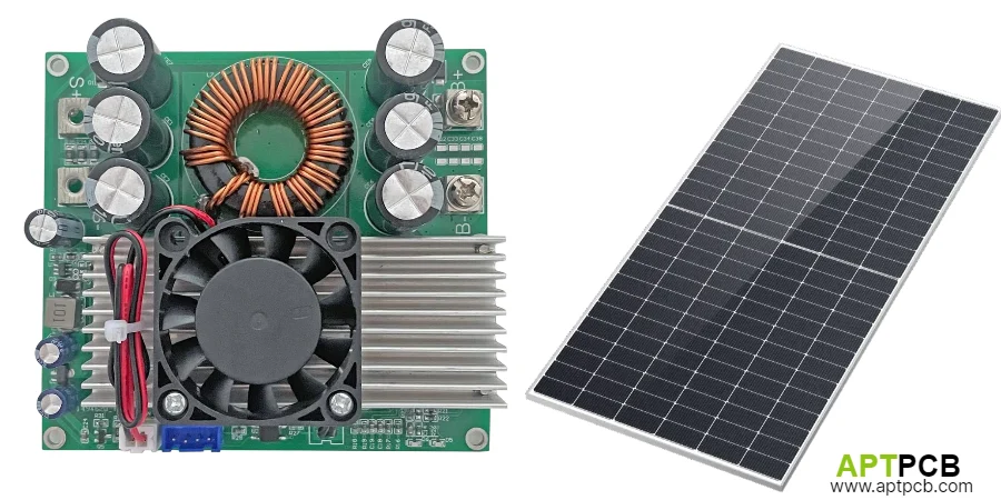
Solar Inverter Control and Power PCB Manufacturing
Solar inverters represent the heart of any photovoltaic system, converting DC power from solar panels into grid-compatible AC power. The complexity of modern inverters requires two distinct PCB types: control boards for intelligence and power boards for energy conversion.
Solar Inverter Control PCB Manufacturer Capabilities
Control PCBs in solar inverters handle complex algorithms for maximum power point tracking, grid synchronization, anti-islanding protection, and communication interfaces. These boards typically feature high-density interconnects, multi-layer stack-ups with controlled impedance, and integration of DSPs or microcontrollers running sophisticated control algorithms.
Manufacturing requirements include:
- HDI technology for dense component placement and fine-pitch BGAs
- Controlled impedance traces for high-speed communication buses
- EMI shielding considerations to prevent interference with power circuits
- Conformal coating compatibility for environmental protection
- IPC Class 3 standards for high-reliability applications
Solar Inverter Power PCB Manufacturer Specifications
Power PCBs in solar inverters must handle high currents and voltages while maintaining efficiency. These boards feature heavy copper layers (4-10 oz), specialized high-temperature materials, and advanced thermal management structures.
Critical manufacturing aspects:
- Heavy copper processing for current-carrying capacity
- Wide trace spacing and clearances for high-voltage isolation
- Thermal vias and copper pours for heat dissipation
- Specialized solder mask for high-voltage applications
- Metal core or IMS substrates for enhanced thermal performance
The integration between control and power boards requires careful attention to signal isolation, EMI management, and thermal zones to ensure reliable operation across the inverter's full power range.
Microinverter PCB Assembly for Distributed Generation
Microinverter pcb assembly represents a paradigm shift in solar system architecture, placing power conversion at each solar panel rather than centralizing it. This distributed approach improves system efficiency, simplifies installation, and enhances monitoring capabilities, but places extreme demands on PCB miniaturization and reliability.
Design Challenges in Microinverter Manufacturing
Microinverters must pack complete DC-AC conversion, MPPT tracking, monitoring, and communication capabilities into a compact enclosure that mounts directly behind solar panels. The PCB assembly must withstand:
- Temperature cycling from -40°C to +85°C ambient
- High humidity and condensation cycles
- Continuous operation at elevated temperatures
- 25-year design life with minimal degradation
Advanced Assembly Techniques for Microinverters
Manufacturing microinverter PCBs requires specialized assembly processes:
- Selective soldering for high-power through-hole components
- Underfill application for flip-chip and BGA components
- Potting and encapsulation for environmental protection
- Automated optical inspection at multiple stages
- In-circuit and functional testing under thermal stress
Component placement accuracy becomes critical when dealing with high-frequency switching circuits in confined spaces. Advanced pick-and-place systems with vision alignment ensure precise positioning of power semiconductors, transformers, and passive components.
MPPT Controller PCB Manufacturing Technologies
Maximum Power Point Tracking (MPPT) represents the intelligence behind efficient solar energy harvesting. As an mppt controller pcb manufacturer, the focus extends beyond basic DC-DC conversion to include sophisticated algorithms that continuously optimize power extraction under varying irradiance and temperature conditions.
Circuit Complexity in MPPT Controllers
MPPT controllers incorporate multiple power conversion stages, measurement circuits, and control algorithms:
- Buck-boost converters with synchronous rectification
- High-resolution ADCs for voltage and current monitoring
- Temperature compensation circuits
- Communication interfaces (RS485, CAN, Ethernet)
- Protection circuits for overvoltage, overcurrent, and reverse polarity
Manufacturing Requirements for MPPT PCBs
The manufacturing process must accommodate:
- Mixed-signal design with careful analog-digital separation
- High-current paths requiring 2-4 oz copper
- Precision component placement for current sensing resistors
- Thermal management features including thermal pads and heat spreaders
- Conformal coating application without affecting heat dissipation
Quality control for MPPT controllers includes parametric testing of conversion efficiency across the full input voltage and current range, ensuring tracking algorithms perform correctly under dynamic conditions.
Solar Charge Controller PCB Assembly Solutions
Solar charge controller pcb assembly serves off-grid and hybrid solar systems, managing battery charging while protecting against overcharge, deep discharge, and reverse current flow. These controllers range from simple PWM designs to sophisticated multi-stage charging systems with battery conditioning features.
PWM vs MPPT Charge Controller Manufacturing
Manufacturing approaches differ significantly between PWM and MPPT charge controllers:
PWM Controllers:
- Simpler 2-4 layer PCB designs
- Focus on robust switching elements
- Cost-optimized BOM and assembly
- Basic protection and indication circuits
MPPT Charge Controllers:
- Complex 6-8 layer stack-ups
- Advanced power conversion topologies
- Precision analog measurement circuits
- Sophisticated thermal management
Assembly Considerations for Charge Controllers
Key assembly requirements include:
- Heavy-duty terminals for battery and panel connections
- Robust conformal coating for humidity protection
- Heat sink attachment with thermal interface materials
- LCD/LED display integration for user interfaces
- Weatherproof enclosure compatibility
Testing protocols must verify charging algorithms, protection thresholds, and temperature compensation across the full operating range.
PV DC Combiner PCB Manufacturing and Safety
PV dc combiner pcb manufacturing addresses the critical junction where multiple solar strings connect before feeding into inverters. These boards must handle high DC voltages (up to 1500V) while providing overcurrent protection, monitoring, and arc fault detection.
High-Voltage Design Considerations
Combiner PCBs face unique challenges:
- Creepage and clearance distances per IEC standards
- Arc-resistant materials and conformal coatings
- Surge protection integration (Type 1/Type 2 SPDs)
- Current monitoring for each string input
- Rapid shutdown compliance for safety codes
Manufacturing Processes for Combiner Boards
Specialized manufacturing requirements:
- Wide trace spacing and slot routing for isolation
- High-voltage testing capabilities (hipot, partial discharge)
- Specialized assembly of surge protection devices
- Conformal coating with high dielectric strength
- Burn-in testing under voltage stress
Quality assurance must verify isolation resistance, dielectric withstand voltage, and arc fault detection sensitivity to ensure safety compliance.
Solar LED Driver PCB Manufacturing Applications
Solar led driver pcb manufacturer capabilities extend solar energy into lighting applications, combining photovoltaic charging with efficient LED driving circuits. These products range from simple garden lights to sophisticated street lighting systems with remote monitoring.
Integration of Solar Charging and LED Driving
Solar LED drivers must efficiently manage:
- MPPT or PWM charging from solar panels
- Battery management for energy storage
- Constant current LED driving with dimming control
- Dusk-to-dawn sensing and timing functions
- Wireless communication for smart city applications
Manufacturing Challenges in Solar LED Systems
Production considerations include:
- Weatherproof assembly for outdoor installation
- Thermal management for LED heat dissipation
- EMC compliance for residential/urban deployment
- Cost optimization for competitive markets
- Modular design for various power ratings
Assembly processes must ensure long-term reliability despite thermal cycling, moisture exposure, and UV degradation common in outdoor lighting applications.
Quality Assurance and Environmental Testing
Solar PCB manufacturing demands rigorous quality assurance protocols that go beyond standard electronics testing. The 25-year service life expectation requires comprehensive validation of both materials and assembly processes.
Environmental Stress Testing Protocols
Critical testing includes:
- Thermal cycling (-40°C to +85°C, 1000+ cycles)
- Damp heat testing (85°C/85% RH, 1000 hours)
- UV exposure testing for outdoor components
- Salt spray testing for coastal installations
- Vibration and mechanical shock testing
Accelerated Life Testing and Reliability
Reliability validation encompasses:
- HALT/HASS testing to identify failure modes
- Power cycling under maximum load conditions
- Insulation resistance monitoring during stress
- Solder joint reliability through cross-sectioning
- Component degradation analysis
Statistical process control and continuous monitoring ensure consistent quality across production runs, with traceability from raw materials through final assembly.
FAQ
What certifications are required for solar PCB manufacturing?
Solar PCB manufacturers typically need ISO 9001 for quality management, UL certification for safety compliance, and IPC standards for manufacturing processes. Additional certifications like TUV for photovoltaic components may be required for specific markets.
How do heavy copper PCBs improve solar inverter performance?
Heavy copper PCBs (4-10 oz) reduce resistive losses, improve current carrying capacity, and enhance thermal dissipation. This results in higher efficiency, better thermal management, and increased reliability in high-power solar inverters.
What makes microinverter PCB assembly more challenging than string inverters?
Microinverters require extreme miniaturization while maintaining high power density, superior thermal management in confined spaces, and enhanced environmental protection for direct panel mounting. The assembly process must achieve automotive-grade reliability in a cost-sensitive market.
Why is conformal coating critical for solar PCBs?
Conformal coating protects against moisture, dust, and chemical contaminants while providing additional insulation for high-voltage circuits. In solar applications, it prevents corrosion, reduces arc fault risk, and extends operational life in harsh outdoor environments.
Conclusion
Solar PCB manufacturing represents a critical enabling technology for the renewable energy transition. From sophisticated solar inverter control pcb manufacturer capabilities to robust solar charge controller pcb assembly, each application demands specialized expertise in materials, processes, and testing. Success requires not just manufacturing capability, but deep understanding of solar system requirements, environmental challenges, and long-term reliability expectations.
As the solar industry continues evolving toward higher efficiencies and lower costs, PCB manufacturers must innovate in materials, processes, and design approaches. The integration of advanced manufacturing techniques with comprehensive quality assurance ensures solar electronic systems meet their promised 25-year operational life while maintaining performance in the world's harshest environments.