Contents
- The Context: What Makes Stackup Documentation Guide Challenging
- The Core Technologies (What Actually Makes It Work)
- Ecosystem View: Related Boards / Interfaces / Manufacturing Steps
- Comparison: Common Options and What You Gain / Lose
- Reliability & Performance Pillars (Signal / Power / Thermal / Process Control)
- The Future: Where This Is Going (Materials, Integration, Ai/automation)
- Request a Quote / DFM Review for Stackup Documentation Guide (What to Send)
- Conclusion
A comprehensive stackup documentation guide is the bridge between theoretical physics in CAD software and the physical reality of the lamination press. It is not merely a list of layers; it is a precise engineering specification that defines material types, dielectric constants, copper weights, and the exact sequence of construction required to achieve signal integrity and mechanical stability.
When done correctly, stackup documentation eliminates the "Engineering Query (EQ)" ping-pong that delays projects by weeks. It ensures that the board built in the prototype phase is identical to the board built in mass production, preserving the delicate balance of impedance, thermal management, and physical flatness.
Highlights
- Translation of Intent: How to convert digital impedance requirements into physical material instructions.
- Material Realities: Understanding the difference between "generic FR4" and specific slash numbers or brands.
- Manufacturing Tolerances: Why the "pressed thickness" differs from the "theoretical thickness" and how to document it.
- Hybrid Constructions: Managing documentation for boards mixing high-speed materials with standard epoxy glass.
- Verification: The role of test coupons and TDR (Time Domain Reflectometry) in validating the documented stackup.
The Context: What Makes Stackup Documentation Guide Challenging
The primary challenge in documenting a PCB stackup lies in the disconnect between the digital design environment and the analog nature of manufacturing. In a CAD tool, a dielectric layer is a fixed number, say 0.1mm. In the factory, that layer is a sheet of "prepreg"—fiberglass cloth impregnated with semi-cured resin—that flows, compresses, and cures under heat and pressure. The final thickness depends on the copper density of the adjacent layers, the resin content of the prepreg, and the lamination cycle used.
If the documentation is rigid and ignores these process variables, the manufacturer cannot build the board to spec. Conversely, if the documentation is too loose, the manufacturer might substitute materials that alter the electrical performance.
Furthermore, the supply chain adds complexity. A designer might specify a niche material from a specific vendor that has a 12-week lead time. A robust stackup documentation guide helps engineers specify "equivalents" based on critical parameters (Tg, Dk, Df) rather than just brand names, allowing manufacturers like APTPCB (APTPCB PCB Factory) to utilize available stock without compromising performance.
Finally, density drives difficulty. As layer counts increase and boards become thinner, the margin for error shrinks. A 10% tolerance on a 4-mil dielectric is much harder to control than on a 10-mil dielectric. Documentation must explicitly state which layers carry impedance-controlled traces so the manufacturer can adjust the prepreg selection to hit the target impedance, rather than just hitting a target overall thickness.
The Core Technologies (What Actually Makes It Work)
Creating a functional stackup requires understanding the building blocks of the PCB. Documentation is essentially a recipe for combining these blocks.
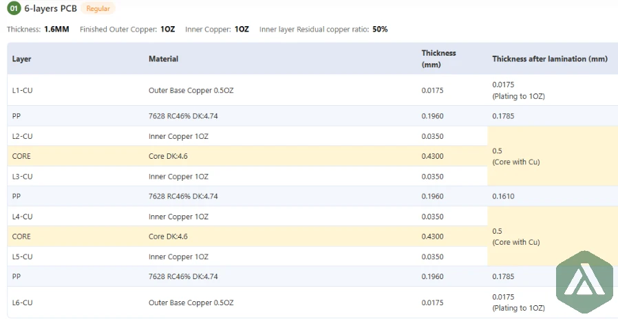
1. Core vs. Prepreg Construction
The fundamental distinction in any PCB stack-up is between the "core" and the "prepreg."
- Cores are fully cured layers of fiberglass and resin with copper foil bonded to both sides. They are rigid and have a known thickness and dielectric constant.
- Prepreg (Pre-impregnated) is the "glue" layer. It is fiberglass with semi-cured (B-stage) resin. During lamination, it melts, flows into the gaps between copper traces, and cures into a solid (C-stage).
- Documentation Criticality: You must specify which layers are cores and which are prepreg. A "foil construction" (starting with outer copper foil and prepreg) behaves differently mechanically than a "core construction."
2. Resin Content and Flow
The percentage of resin in the prepreg determines how much "fill" is available for the copper pattern.
- High Resin Content: Good for filling heavy copper layers but may have a higher coefficient of thermal expansion (CTE).
- Glass Weave Style: The documentation should sometimes specify glass styles (e.g., 1080, 2116, 7628). Tighter weaves (like 1080 or 106) provide more consistent impedance for high-speed signals but are thinner. Open weaves (like 7628) are cheaper and thicker but can cause "fiber weave effect" signal skew.
- The Trade-off: If you don't document the glass style, the factory will use the most economical option, which might not support your 10Gbps interface.
3. Copper Balancing and Weight
Copper is not just an electrical conductor; it is a structural element.
- Warpage Control: The stackup must be symmetrical around the center axis. If Layer 2 is a solid ground plane and Layer 3 is a sparse signal layer, the board will warp during reflow. Documentation should enforce symmetry in both copper weight and dielectric thickness.
- Plating Allowance: Documentation must distinguish between "Base Copper" (start weight) and "Finished Copper" (after plating). A common error is specifying "1 oz finished" on an inner layer, which usually means starting with 1 oz foil, whereas on outer layers, "1 oz finished" usually starts with 0.5 oz foil and adds plating.
4. Impedance Control Structures
For high-speed designs, the stackup is the tuning fork.
- Reference Planes: The distance between the signal trace and the reference plane (GND) dictates impedance.
- Calculation vs. Reality: Designers use impedance calculators to estimate trace widths. However, the documentation should list the target impedance (e.g., 50Ω ±10%) rather than just fixed trace widths. This allows the CAM engineer to make micro-adjustments to the trace width (e.g., ±0.5 mil) to compensate for the actual batch of dielectric material used.
Ecosystem View: Related Boards / Interfaces / Manufacturing Steps
The stackup document does not exist in a vacuum; it ripples through every stage of manufacturing and assembly.
Impact on Drilling and Plating: The "Aspect Ratio" is the ratio of the board thickness to the smallest drilled hole. A thick stackup with tiny vias creates a high aspect ratio, making it difficult to plate copper into the hole barrels.
- Documentation Link: If your stackup results in a 3mm thick board, you cannot easily use 0.2mm mechanical drills. You may need to specify HDI PCB technology with laser microvias, which changes the lamination sequence entirely (sequential lamination).
Impact on Assembly (PCBA): The choice of materials in the stackup affects how the board behaves in the soldering oven.
- CTE Mismatch: If the stackup uses materials with different thermal expansion rates (e.g., a hybrid stackup with Rogers and FR4), the stresses during reflow can delaminate the board or crack solder joints.
- Flatness: As mentioned, unbalanced stackups lead to bow and twist. Automated pick-and-place machines require flat boards. Documentation that ignores copper balance often results in boards that are rejected at the SMT assembly stage.
Impact on Signal Integrity: The stackup defines the "loss tangent" (Df) of the transmission line.
- Material Selection: For RF or high-speed digital, standard FR4 acts like a sponge for signals, absorbing energy. Documentation must specify "Low Loss" or "Ultra Low Loss" materials.
- Interface Standards: Interfaces like PCIe Gen 5 or DDR5 have strict loss budgets. The stackup documentation is the primary control knob for meeting these budgets.
Comparison: Common Options and What You Gain / Lose
Engineers often face a choice between generic specifications (cheaper, faster) and rigid, specific stackups (consistent, potentially expensive). Understanding the trade-offs helps in making the right decision for the product lifecycle.
Generic "Pool" Stackups: Many prototype shops offer a "standard" stackup. You design to their numbers, and they guarantee the impedance.
- Pros: Fast, cheap, no custom engineering.
- Cons: You are locked into their specific material set. Moving to a different vendor later requires a redesign.
Custom "Spec-Driven" Stackups: You define the layer count and performance targets (e.g., "6 layers, 1.6mm, 50Ω on L1/L3"). You allow the vendor to propose the exact construction.
- Pros: Flexible supply chain. The vendor optimizes for their stock and press capabilities.
- Cons: Requires a DFM review cycle to finalize the exact build.
Rigid "Material-Driven" Stackups: You specify "Isola 370HR, 2x1080 prepreg, 1 oz foil."
- Pros: Absolute control. The physics are fixed.
- Cons: High risk of supply chain disruption. If that specific prepreg is out of stock, the project stalls.
Decision Matrix: Technical Choice → Practical Outcome
| Technical choice | Direct impact |
|---|---|
| Specifying "IPC-4101/126" (Generic High Tg) | Allows factory to use any qualified brand (Shengyi, ITEQ, Isola). Lowers cost and lead time. |
| Specifying exact glass weave (e.g., 106 vs 7628) | Ensures consistent impedance and skew control but may force the factory to order non-standard stock. |
| Defining "Foil Construction" (Outer layers are foil) | Standard for HDI and cost-efficiency. Allows smoother outer copper for fine pitch components. |
| Defining "Core Construction" (Outer layers are core) | Older method, rarely used now except for specific military/legacy reliability requirements. Higher cost. |
Reliability & Performance Pillars (Signal / Power / Thermal / Process Control)
A stackup document is not just about dimensions; it is a reliability contract.
1. Thermal Reliability (Tg and Td)
The Glass Transition Temperature (Tg) is where the resin turns from hard to soft. The Decomposition Temperature (Td) is where it physically breaks down.
- Documentation: For lead-free soldering (which requires higher temps), the stackup must specify High-Tg materials (typically >170°C). If you document "Standard FR4" (Tg 130°C) for a complex board, the Z-axis expansion during reflow will likely rip the copper plating off the via walls (barrel cracks).
2. Signal Integrity (Dk and Df)
- Dk (Dielectric Constant): Determines signal speed and impedance. It varies with frequency. Good documentation specifies the Dk at the operating frequency (e.g., "Dk 3.8 @ 10GHz").
- Df (Dissipation Factor): Determines signal loss. For long traces on server backplanes, you need materials with very low Df (e.g., <0.005).
3. Caf Resistance (Conductive Anodic Filament)
In high-voltage or high-density applications, copper dendrites can grow along the glass fibers, causing shorts.
- Mitigation: Stackup documentation can specify "CAF Resistant" materials. This ensures the resin chemistry and glass interface are designed to prevent this growth.
4. Process Control and Verification
How do you know the factory followed the stackup?
- Test Coupons: The documentation should require impedance coupons. These are small PCB sections built on the panel rails that mimic the actual traces.
- Microsectioning: For critical builds, require a microsection report. This involves cutting a sample board and measuring the actual dielectric thicknesses under a microscope to verify they match the stackup drawing.
The Future: Where This Is Going (Materials, Integration, Ai/automation)
The era of static PDF stackup drawings is fading. The future lies in intelligent data exchange and advanced material integration.
Hybrid and Embedded Technologies: We are seeing more "Hybrid Stackups" where expensive PTFE materials (like Rogers) are used only on the high-speed layers, while standard FR4 is used for power and ground to save cost. Documenting these requires careful attention to the resin flow compatibility between different material families. Furthermore, embedded capacitance and resistance materials are being integrated directly into the stackup, requiring the documentation to define passive component layers.
AI-Driven Stackup Generators: Software is evolving to automatically generate stackups based on a library of available materials and design constraints. Instead of a designer guessing a construction, they input "12 layers, 1.6mm, 50/90/100 Ohm targets," and the software proposes a valid construction using materials currently in stock at the preferred vendor. This "Digital Twin" approach reduces the DFM cycle from days to minutes.
5-Year Performance Trajectory (Illustrative)
| Performance metric | Today (typical) | 5-year direction | Why it matters |
|---|---|---|---|
| Dielectric Thickness | 3 mil (75 micron) min | 1 mil (25 micron) standard | Enables ultra-high-density interconnects (HDI) for mobile and AI chips. |
| Material Data Exchange | PDF / Excel / Text notes | IPC-2581 / ODB++ integrated stackup data | Eliminates manual data entry errors and speeds up NPI. |
| Layer Count (High End) | 20-30 layers | 40-60+ layers becoming common | Required for massive parallel processing in AI servers and switches. |
Request a Quote / DFM Review for Stackup Documentation Guide (What to Send)
When requesting a quote or a DFM review for a complex stackup, clarity is your best currency. Providing a complete data package allows APTPCB to validate your design against actual material stocks and press capabilities immediately, rather than guessing your intent.
Checklist for a Perfect Stackup Request:
- Layer Count & Finished Thickness: State the target (e.g., 1.6mm ±10%) and whether it includes plating/solder mask.
- Material Requirements: Specify Tg (e.g., >170°C), Dk/Df requirements, or specific brands (e.g., "Isola 370HR or equivalent").
- Impedance Table: List every controlled impedance trace (Layer, Reference Layers, Target Ohms, Trace Width/Space).
- Copper Weights: Define base copper for all layers (e.g., "Outer 0.5oz / Inner 1oz").
- Via Structure: Clearly define blind, buried, and through-hole via spans.
- Special Constraints: Note any requirements for sequential lamination, back-drilling, or resin-filled vias.
- Acceptance Criteria: Specify if you require IPC Class 2 or Class 3, and if cross-section reports are needed.
Conclusion
Stackup documentation is the blueprint of the PCB's physical soul. It transforms a schematic's electrical potential into a manufacturable reality. By moving away from ambiguous notes and embracing detailed, material-aware specifications, designers can