Contents
- The Context: What Makes Stencil Thickness Basics Challenging
- The Core Technologies (What Actually Makes It Work)
- Ecosystem View: Related Boards / Interfaces / Manufacturing Steps
- Comparison: Common Options and What You Gain / Lose
- Reliability & Performance Pillars (Signal / Power / Thermal / Process Control)
- The Future: Where This Is Going (Materials, Integration, Ai/automation)
- Request a Quote / DFM Review for Stencil Thickness Basics (What to Send)
- Conclusion
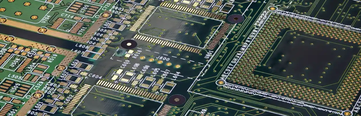
In the world of Surface Mount Technology (SMT), stencil thickness basics refer to the fundamental parameters that dictate how much solder paste is deposited onto a PCB pad. It is not merely about choosing a sheet of metal; it is about calculating the precise volume of paste required to form a reliable mechanical and electrical joint without causing shorts. A "good" stencil design balances the conflicting needs of large power components (which crave volume) and microscopic passives (which demand precision), ensuring high yield and long-term reliability.
Highlights
- Volume Control: Thickness is the primary lever for determining the theoretical volume of solder paste ($Volume = Area \times Thickness$).
- Area Ratio Rule: For paste to release from the aperture, the area ratio (aperture opening area vs. aperture wall area) must generally exceed 0.66.
- The "Goldilocks" Conflict: Fine-pitch parts need thinner stencils to prevent bridging; large connectors need thicker stencils for mechanical strength.
- Material Impact: Stainless steel is standard, but nickel electroforming or nano-coatings can alter effective release properties.
- Step Stencils: Advanced manufacturing allows for variable thickness on a single foil to accommodate mixed-technology boards.
The Context: What Makes Stencil Thickness Basics Challenging
The fundamental challenge in selecting the right stencil thickness lies in the diversity of modern electronics. A decade ago, a board might have been populated entirely with 0805 passives and SOIC packages, allowing for a uniform, thick stencil (e.g., 0.15mm or 6 mil). Today, a single PCB often integrates a massive power inductor requiring significant solder volume alongside a 0.4mm pitch BGA or 01005 capacitors that require microscopic deposits.
This creates a physical contradiction. If you select a thick stencil (0.15mm) to satisfy the power inductor, the apertures for the fine-pitch BGA become deep, narrow wells. The solder paste, which is a sticky suspension of metal spheres and flux, tends to stick to the walls of these deep apertures rather than releasing onto the pad. This results in "insufficient solder" or clogged apertures. Conversely, if you choose a thin stencil (0.10mm or 4 mil) to ensure excellent release for the BGA, the power inductor receives too little paste, leading to weak joints that may crack under thermal cycling or mechanical stress.
At APTPCB (APTPCB PCB Factory), we often see designs where the layout is perfect, but the assembly yield suffers because the stencil strategy was an afterthought. The difficulty is compounded by lead time pressures; changing a stencil requires ordering a new laser-cut foil, which halts production. Therefore, understanding the basics of thickness and aperture design during the DFM (Design for Manufacturability) phase is critical for avoiding costly line-down situations.
The Core Technologies (What Actually Makes It Work)
To master stencil thickness basics, one must look beyond the metal foil itself and understand the physics of paste transfer. Several core technologies and mathematical principles govern whether the paste will print successfully.
1. The Aspect and Area Ratios
The physics of printing is governed by the battle between the surface tension of the paste on the PCB pad and the friction of the paste against the stencil walls.
- Aspect Ratio: The width of the aperture divided by the thickness of the stencil ($W / T$). This should generally be greater than 1.5.
- Area Ratio (The Golden Rule): The area of the aperture opening divided by the area of the aperture side walls.
- Formula: $Area Ratio = (L \times W) / (2 \times (L + W) \times T)$
- Threshold: For standard stainless steel stencils, the Area Ratio must be > 0.66. If it drops below this, the paste will likely stick inside the stencil aperture rather than depositing on the board.
2. Laser Cutting vs. Electroforming
How the stencil is made affects the smoothness of the aperture walls, which in turn influences the effective thickness choice.
- Laser Cut Stainless Steel: The industry standard. A laser cuts the apertures from a steel sheet. Post-processing (electropolishing) is often used to smooth the micro-burrs left by the laser, improving paste release.
- Electroformed (E-Fab): Instead of cutting, nickel is grown atom-by-atom around a mandrel. This creates perfectly smooth, tapered walls that release paste much better than laser-cut steel. This technology allows engineers to use slightly thicker stencils for fine-pitch parts because the release efficiency is higher.
3. Step-Stencil Technology
When a single thickness cannot satisfy all components, "Step Stencils" are the technological solution.
- Step-Down: The base foil is thick (e.g., 0.15mm) for the majority of the board, but specific areas around fine-pitch components are milled down to a thinner gauge (e.g., 0.12mm or 0.10mm).
- Step-Up: The base foil is thin, and additional material is added (or the foil is thicker and the majority is milled down) to provide extra volume for specific heavy-duty connectors.
For complex designs involving HDI PCB layouts, step stencils are often the only viable path to zero-defect manufacturing.
Ecosystem View: Related Boards / Interfaces / Manufacturing Steps
Stencil thickness does not exist in a vacuum. It interacts directly with the PCB surface finish, the solder paste chemistry, and the placement equipment.
The Surface Finish Interaction
The flatness of the PCB pads dramatically affects how the stencil sits on the board (the "gasketing" effect).
- HASL (Hot Air Solder Leveling): This finish leaves a domed, irregular surface. A stencil cannot seal perfectly against a HASL pad, leading to paste squeezing out underneath the stencil (bridging). If using HASL, engineers often reduce stencil thickness or aperture size to compensate for this lack of gasketing.
- ENIG (Electroless Nickel Immersion Gold) & OSP: These finishes are perfectly flat. The stencil can sit flush against the pads, creating a tight seal. This allows for more precise volume control and typically supports the use of standard thickness calculations without aggressive compensation.
Solder Paste Particle Size
The "Type" of solder paste refers to the size of the metal spheres suspended in the flux.
- Type 3: Standard for most assemblies.
- Type 4 & 5: Used for fine-pitch components. If you are forced to use a very thin stencil (e.g., 0.08mm) with tiny apertures, you must use Type 4 or Type 5 paste. Large spheres (Type 3) can clog small apertures, effectively changing the "effective" thickness to zero because nothing prints.
The Feedback Loop: SPI
Solder Paste Inspection (SPI) machines measure the actual volume of paste deposited. They are the ultimate judge of whether your stencil thickness choice was correct. If the SPI consistently reports "insufficient volume" on a QFN center pad, the solution might not be a thicker stencil, but rather a segmented aperture design to prevent "scooping" (where the squeegee blade dips into a large aperture and scoops paste out).
Comparison: Common Options and What You Gain / Lose
When specifying a stencil for a standard mixed-technology board, engineers usually choose between three standard thicknesses: 0.10mm (4 mil), 0.12mm (5 mil), and 0.15mm (6 mil). Each represents a trade-off between resolution and power handling.
Decision Matrix: Technical Choice → Practical Outcome
| Technical choice | Direct impact |
|---|---|
| 0.10mm (4 mil) Foil | Excellent for 0.4mm pitch BGAs and 0201s. Risk of insufficient solder on large connectors or shielding cans. |
| 0.12mm (5 mil) Foil | The industry "sweet spot." Balances fine pitch (down to 0.5mm) with adequate volume for standard passives and ICs. |
| 0.15mm (6 mil) Foil | Ideal for power boards, heavy copper, and large connectors. High risk of bridging on any component with pitch < 0.65mm. |
| Nano-Coated Foil | Increases transfer efficiency by 10-20%. Allows using a thinner stencil while maintaining volume, or cleaner release on fine pitch. |
Reliability & Performance Pillars (Signal / Power / Thermal / Process Control)
The thickness of the stencil directly influences the reliability of the final PCBA. It is not just about passing visual inspection; it is about the longevity of the joint.
Thermal Reliability and Solder Volume
For power components like MOSFETs or QFN thermal pads, the solder joint transfers heat to the PCB. If the stencil is too thin, the solder layer will be insufficient to handle the thermal expansion mismatch between the component and the board. This leads to early fatigue cracks. Conversely, excessive thickness on a thermal pad can cause the component to "float" or tilt, disconnecting the signal pins. A common rule is to reduce the aperture area on large thermal pads by 20-50% (window-pane design) to control this, rather than just relying on thickness.
Signal Integrity and Flux Residue
In high-frequency applications, excess solder paste can be detrimental. Large fillets can act as capacitive stubs. Furthermore, if a stencil is too thick and causes bridging under a component (like a BGA), it creates a short that is invisible to visual inspection and requires X-ray to detect. Even if it doesn't short, excess flux residue trapped under low-standoff components can cause leakage currents in humid environments.
Process Control: The Transfer Efficiency
Reliability is also about repeatability. A stencil aperture with a borderline Area Ratio (e.g., 0.60) might print perfectly 80% of the time and fail 20% of the time depending on humidity and paste viscosity. This variation is unacceptable in mass production. By adhering to strict thickness/aperture rules, APTPCB ensures that the "Transfer Efficiency" remains close to 100%—meaning the volume of paste on the board matches the volume of the aperture.
| Metric | Acceptance Criteria |
|---|---|
| Solder Volume | ±50% of theoretical aperture volume (per IPC-7527). |
| Alignment | Paste must be at least 70% on the pad. |
| Height | Paste height should be uniform; spikes indicate poor release. |
| Bridging | Zero bridging allowed between pads. |
The Future: Where This Is Going (Materials, Integration, Ai/automation)
As components shrink to 008004 sizes and power densities rise, the "one thickness fits all" approach is becoming obsolete. The industry is moving toward adaptive and highly engineered stencil solutions.
5-Year Performance Trajectory (Illustrative)
| Performance metric | Today (typical) | 5-year direction | Why it matters |
|---|---|---|---|
| **Variable Thickness** | Step stencils (milled/etched). | 3D printed stencils / Jet printing. | Allows infinite volume variation per pad without expensive step manufacturing. |
| **Aperture Coating** | Nano-coating (optional). | Standard integrated self-cleaning surfaces. | Reduces under-stencil wiping frequency, increasing line throughput. |
| **Process Feedback** | SPI data alerts operator. | AI auto-corrects printer pressure/speed. | Eliminates human error in tuning print parameters for specific thicknesses. |
Request a Quote / DFM Review for Stencil Thickness Basics (What to Send)
When you are ready to move from design to assembly, the quality of your data determines the quality of the stencil. At APTPCB, we can optimize the stencil design for you, but providing clear intent helps us move faster.
- Gerber Files: Specifically the Paste Top (GTP) and Paste Bottom (GBP) layers.
- Panelization: If you are ordering the stencil for a panel, send the panelized data, not just the single unit.
- Component List: Highlight any critical fine-pitch parts (0.4mm BGA, 0201s) or heavy power connectors.
- Thickness Preference: State if you have a standard (e.g., "Use 5 mil unless DFM suggests otherwise").
- Fiducials: Ensure fiducial marks are clear on the paste layer (usually half-etched) for machine alignment.
- Frame Size: Specify if you need a standard 29"x29" frame or a frameless foil for a tensioning system.
- Solder Mask Type: Mention if you are using defined pads (SMD) or non-solder mask defined (NSMD), as this affects aperture scaling.
Conclusion
Stencil thickness basics are the foundation of SMT yield. It is a variable that seems static but interacts dynamically with every other part of the assembly process—from the PCB surface finish to the thermal profile of the reflow oven. A choice that is "good enough" for a prototype might cause 5% fallout in mass production if the Area Ratios are ignored.
By understanding the trade-offs between release efficiency and solder volume, and by leveraging technologies like step stencils and nano-coatings, you can ensure robust, reliable solder joints. Whether you are building high-density consumer electronics or rugged industrial power boards, APTPCB is equipped to guide you through the DFM process, ensuring your stencil thickness is optimized for first-pass success.