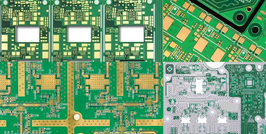
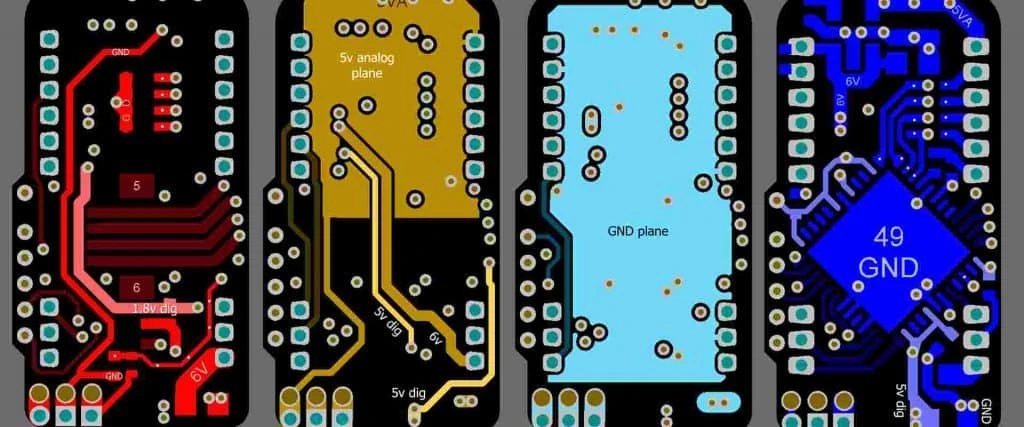
Designing a superconducting qubit control PCB requires navigating physics that do not exist at room temperature. These boards operate inside dilution refrigerators at millikelvin (mK) temperatures, where standard dielectric constants shift, copper resistance drops significantly (or becomes superconducting), and magnetic impurities can destroy quantum coherence. APTPCB (APTPCB PCB Factory) specializes in fabricating these high-precision interconnects where thermal budgets and signal integrity are strictly limited.
Quick Answer (30 seconds)
- Eliminate Magnetic Materials: Standard ENIG or ENEPIG finishes contain nickel, which is magnetic and disrupts qubit coherence. Use Immersion Silver, Soft Gold (direct on copper), or non-magnetic specific plating.
- Account for Cryogenic $D_k$ Shift: Substrate dielectric constants decrease at 4K compared to 300K. Simulate impedance using cryogenic material data, not room-temperature datasheets.
- Thermalization is Critical: Signal traces must not conduct excessive heat from higher temperature stages (4K) to the mixing chamber (10-20mK). Use specific trace geometries or superconducting materials (like Niobium or Aluminum) where applicable.
- Connector Reliability: SMPM or GPPO connectors must withstand thermal cycles without cracking solder joints due to Coefficient of Thermal Expansion (CTE) mismatches.
- Surface Roughness: At microwave frequencies (4-8 GHz), copper roughness increases loss. Use VLP (Very Low Profile) or HVLP copper foils.
- Cleanliness: Flux residues and oxidation are fatal to high-Q resonators. Strict cleaning protocols are mandatory.
When superconducting qubit control PCB applies (and when it doesn’t)
Use this technology when:
- You are routing signals to/from a quantum processor inside a cryostat or dilution refrigerator.
- The operating temperature is below 4 Kelvin (liquid helium range) or down to millikelvin levels.
- Signal frequencies range from DC to 12+ GHz (typically 4-8 GHz for qubit readout/control).
- You require a cryostat feedthrough PCB to bridge temperature stages (e.g., 300K to 50K, or 4K to mK).
- Magnetic hygiene is a strict requirement to prevent decoherence.
Do not use this technology when:
- The application is standard room-temperature RF communication (use standard High Frequency PCB processes instead).
- Magnetic materials (Nickel, Iron) are acceptable in the signal path.
- High power transmission is required (superconducting traces have low critical current limits).
- Cost is the primary driver over performance; these boards require specialized materials and handling.
Rules & specifications

Cryogenic environments are unforgiving. A single violation of these rules can render a quantum experiment useless.
| Rule | Recommended Value/Range | Why it matters | How to verify | If ignored |
|---|---|---|---|---|
| Surface Finish | Immersion Silver, OSP, or Direct Soft Gold (No Nickel) | Nickel is ferromagnetic and causes magnetic vortices/decoherence. | XRF analysis to confirm 0% Ni content. | Qubit coherence times ($T_1$, $T_2$) drop drastically. |
| Dielectric Material | Rogers 4003C, 3003, or Kapton (Flex) | Low loss tangent ($\tan \delta$) and stable CTE at cryogenic temps. | Review Rogers PCB materials data sheets for cryogenic curves. | Impedance mismatch due to $D_k$ shift; mechanical cracking. |
| Trace Impedance | $50\Omega \pm 2\Omega$ (Single), $100\Omega \pm 5\Omega$ (Diff) | Reflections cause standing waves that heat the fridge and corrupt pulses. | TDR measurement (Time Domain Reflectometry). | Signal reflection; poor qubit fidelity. |
| Copper Type | Rolled Annealed or Electrodeposited (VLP) | Smooth copper reduces skin effect losses at microwave frequencies. | Profilometer check on raw laminate. | Higher insertion loss; signal attenuation. |
| Thermal Vias | Minimized or Superconducting filled | Standard copper vias conduct heat. Superconducting vias block heat but pass current. | Thermal modeling of the stackup. | Fridge fails to reach base temperature (mK). |
| Solder Mask | Removed on signal lines (or totally removed) | Solder mask is lossy and hygroscopic. | Visual inspection. | Increased dielectric loss; outgassing in vacuum. |
| CTE Matching | X/Y axis: 16-17 ppm/°C (match Copper) | Prevents delamination during cool-down from 300K to 0.01K. | TMA (Thermomechanical Analysis). | Board delamination; open circuits after cooling. |
| Connector Torque | Specific to SMPM/SMA (e.g., 0.2-0.5 Nm) | Over-torquing cracks cold solder joints; under-torquing fails at cold. | Torque wrench calibration. | Intermittent connections during thermal cycling. |
| Flux Residue | IPC Class 3 Cleanliness or better | Residues become dielectric losses and noise sources. | Ion chromatography test. | Noisy measurements; reduced resonator Q-factor. |
| Grounding | Dense stitching vias ($\lambda/20$ spacing) | Prevents cavity resonances within the substrate. | EM Simulation (HFSS/CST). | Crosstalk between control lines. |
Implementation steps

Follow this sequence to ensure your superconducting qubit control PCB functions correctly at millikelvin temperatures.
Define the Thermal Budget Calculate the maximum allowable heat load for the specific fridge stage (e.g., 10 $\mu W$ at the mixing chamber). This dictates the trace width, copper thickness (0.5 oz vs 1 oz), and substrate choice.
Select Cryogenic-Compatible Materials Choose substrates like Rogers RO4003C or specific Polyimide variants for cryostat feedthrough PCB applications. Avoid FR4 entirely due to high loss and poor thermal stability. Consult APTPCB engineering for current stock of non-magnetic laminates.
Simulate with Cryogenic Parameters Adjust your stackup simulation. The dielectric constant ($D_k$) of PTFE-based materials typically drops by 1-2% as the material cools to 4K. Design the trace width for the cold impedance, not the room temperature impedance.
Route for Differential Microwave Signals Implement differential microwave routing cryogenic strategies. Use tight coupling for differential pairs to reject common-mode noise. Ensure length matching is precise (< 0.1mm) to maintain phase coherence of microwave pulses.
Apply Non-Magnetic Surface Finish Specify "No Nickel" explicitly in fabrication notes. Request Immersion Silver (ImmAg) or Direct Gold. Ensure the fabrication house cleans the copper thoroughly before plating to prevent oxidation issues.
Fabrication and Etching Execute etching with tight tolerances ($\pm 0.5$ mil or better). For superconducting traces (e.g., Niobium sputtered on Silicon, or specialized PCB laminates), cleanroom processing is required to prevent contamination.
Assembly with Low-Temperature Solders Use Indium-based solders or specific lead-free alloys that remain ductile at cryogenic temperatures. Standard SAC305 can become brittle.
Validation (Room Temp & Cold) Perform DC continuity checks and VNA (Vector Network Analyzer) sweeps at room temperature. Note that resistance will drop (or vanish) at cold, so room temp checks only validate connectivity, not final performance.
Failure modes & troubleshooting
| Symptom | Likely Cause | Diagnostic Check | Fix / Prevention |
|---|---|---|---|
| High Insertion Loss | Dielectric loss or rough copper | Measure $S_{21}$ with VNA. Check if mask was left on traces. | Use VLP copper; remove solder mask from RF paths. |
| Resonance Frequency Shift | $D_k$ change at low temp | Compare room temp resonance vs. cold resonance. | Model the $\Delta D_k$ (approx -2% for PTFE) during design. |
| Open Circuit at Cold | Via barrel crack (CTE mismatch) | DC resistance check while cooling (monitor continuously). | Use Flex PCB materials or high-reliability via fills; avoid thick boards. |
| Qubit Decoherence | Magnetic impurities | Measure $T_1$ times. Check plating spec. | Switch to non-magnetic plating; verify connector body materials (Brass/BeCu, no Nickel). |
| Thermal Runaway | Excessive heat conduction | Fridge thermometer readings rise. | Reduce copper cross-section; use thermal breaks or superconducting traces. |
| Crosstalk | Poor grounding / Spacing | Measure $S_{41}$/$S_{31}$. | Increase trace separation; add ground stitching vias ("picket fence"). |
Design decisions
Rigid vs. Flex vs. Rigid-Flex For interconnects bridging different temperature stages (e.g., 4K to mK), cryostat feedthrough PCB designs often utilize Rigid-Flex PCB technology. The flexible polyimide section reduces thermal conduction due to its thin profile, while the rigid sections support high-density connectors.
Connector Selection Standard SMA connectors are too bulky for high-qubit-count processors. SMP, SMPM, and multi-coax connectors are preferred. Ensure the connector body is non-magnetic (passivated stainless steel or gold-plated beryllium copper) and the detent force is appropriate for the vibration environment of the pulse tube.
Superconducting Traces In some advanced designs, the PCB traces themselves must be superconducting. This involves specialized substrates (like Silicon or Sapphire) or plating standard copper with superconducting solder (SnPb or InPb) to reduce resistance to zero below the critical temperature ($T_c$).
FAQ
Q: Can I use standard FR4 for superconducting qubit control PCBs? A: No. FR4 has a high loss tangent at microwave frequencies and its thermal expansion properties are unpredictable at cryogenic temperatures, leading to mechanical failure.
Q: Why is nickel forbidden in these PCBs? A: Nickel is ferromagnetic. Even thin layers of nickel in plating (like ENIG) distort the magnetic field homogeneity required for qubit operation, causing rapid decoherence.
Q: How do I handle the impedance change from room temp to cryogenic temp? A: Design for the cold condition. Since $D_k$ decreases, traces designed for $50\Omega$ at 300K might become $52\Omega$ at 20mK. It is often better to be slightly capacitive at room temp so the line hits $50\Omega$ at operating temperature.
Q: What is the lead time for these specialized boards? A: Due to non-standard materials (Rogers/Taconic) and strict non-magnetic processing requirements, lead times are typically longer than standard boards. Special PCB Manufacturing services usually require 2-4 weeks depending on material stock.
Q: Do I need backdrilling for these PCBs? A: Yes. For high-frequency signals (4-8 GHz and above), via stubs act as antennas or filters. Backdrilling removes the unused portion of the via to preserve signal integrity.
Glossary (key terms)
| Term | Definition |
|---|---|
| Dilution Refrigerator | A cryogenic device that provides continuous cooling to temperatures as low as 2mK, used to house quantum processors. |
| Decoherence | The loss of quantum information due to interaction with the environment (noise, heat, magnetic fields). |
| $D_k$ (Dielectric Constant) | A measure of a material's ability to store electrical energy. It changes with temperature, affecting impedance. |
| Loss Tangent ($\tan \delta$) | A measure of signal power lost as heat in the dielectric material. Lower is better. |
| CTE (Coefficient of Thermal Expansion) | The rate at which a material expands or contracts with temperature changes. Mismatches cause cracks. |
| Superconductivity | A state where a material conducts electricity with zero resistance below a critical temperature ($T_c$). |
| Cryostat Feedthrough | An interface that allows electrical signals to pass between different temperature zones in a cryostat while maintaining vacuum and thermal isolation. |
| ENEPIG | Electroless Nickel Electroless Palladium Immersion Gold. Standard ENEPIG is magnetic; "Non-magnetic ENEPIG" uses specific chemistry but is rare. |
| Skin Effect | The tendency of AC current to flow near the surface of a conductor. At mK temps, the anomalous skin effect can alter losses. |
| Thermal Anchoring | Mechanical techniques to ensure cables and PCBs are at the same temperature as the fridge stage they are mounted to. |
Request a quote
For superconducting qubit control PCB projects, standard online auto-quotes are often insufficient due to the strict material and plating requirements.
To get an accurate DFM review and quote, please provide:
- Gerber Files: RS-274X format preferred.
- Stackup Drawing: Specify dielectric materials and copper weights explicitly.
- Fabrication Notes: Clearly state "NO NICKEL PLATING" and "CRYOGENIC APPLICATION."
- Impedance Requirements: List target impedance and frequency (e.g., 50Ω @ 6 GHz).
- Volume: Prototype quantity (usually 5-10 pcs) vs. production.
Contact APTPCB directly if you need assistance selecting the right non-magnetic stackup for your quantum application.
Conclusion
A superconducting qubit control PCB is the critical bridge between room-temperature electronics and the quantum processor. Success depends on rigorous control of magnetic materials, precise impedance matching for differential microwave routing cryogenic signals, and robust thermal management. By adhering to these specialized design rules and partnering with an experienced manufacturer like APTPCB, you ensure your hardware supports, rather than hinders, quantum coherence.