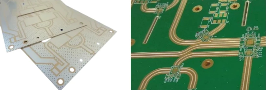
A Sweep Generator PCB is the core hardware responsible for producing a frequency-modulated signal that varies linearly or logarithmically over time. Unlike a fixed-frequency source, this board must maintain amplitude stability and signal purity across a dynamic range, making it essential for testing frequency response in filters, amplifiers, and antennas. Designing these boards requires strict adherence to impedance control, thermal stability, and noise suppression to prevent signal distortion during the sweep.
Sweep Generator PCB quick answer (30 seconds)
Successful manufacturing of a Sweep Generator PCB relies on controlling the signal path and power integrity.
- Impedance Control: Maintain strict 50Ω (or 75Ω) impedance on all RF traces to prevent reflections that distort the sweep envelope.
- Power Isolation: Use ultra-low noise LDOs for Voltage Controlled Oscillators (VCOs); power supply noise directly converts to phase noise.
- Thermal Management: Frequency drift is common; ensure thermal vias and heatsinks are placed under active RF components.
- Shielding: Isolate the Analog Generator PCB sections from digital control logic to prevent spurious emissions.
- Material Selection: Use high-frequency laminates (like Rogers or Teflon) if the sweep range exceeds 1 GHz to minimize dielectric loss.
- Grounding: Employ extensive via stitching around the board edge and between circuit blocks to suppress EMI.
When Sweep Generator PCB applies (and when it doesn’t)
Understanding the specific use case ensures you do not over-engineer or under-spec the board.
Applies when:
- Frequency Response Testing: You need to characterize the bandwidth of a device under test (DUT) using a continuous chirp.
- Radar Systems: The application requires Frequency Modulated Continuous Wave (FMCW) signals for range detection.
- Audio Analysis: An Audio Generator PCB is needed to sweep from 20Hz to 20kHz to test speaker linearity.
- Calibration Equipment: A Calibration Generator is required to verify the performance of spectrum analyzers or receivers.
- Network Analysis: The system acts as the source for a Vector Network Analyzer (VNA).
Does not apply when:
- Fixed Clocking: A standard Clock Generator PCB is sufficient for digital timing where frequency modulation is undesirable.
- Digital Pattern Generation: A BER Generator PCB (Bit Error Rate) focuses on digital data streams rather than analog frequency sweeps.
- High Power Transmission: If the goal is purely power delivery rather than signal analysis, a standard amplifier board is more appropriate.
- Simple Tone Generation: A basic oscillator circuit is cheaper and smaller if only a single sine wave is needed.
Sweep Generator PCB rules and specifications (key parameters and limits)
To ensure the sweep signal remains linear and clean, specific design rules must be followed during layout and fabrication.
| Rule | Recommended Value/Range | Why it matters | How to verify | If ignored |
|---|---|---|---|---|
| Trace Impedance | 50Ω ±5% (or 75Ω) | Prevents signal reflections and standing waves. | TDR (Time Domain Reflectometry) | Signal loss, ripples in sweep amplitude. |
| Dielectric Material | Dk < 3.5, Df < 0.003 (for >1GHz) | Reduces signal attenuation at high frequencies. | Material Datasheet / Stackup Report | High insertion loss, heating of traces. |
| Via Stitching | < λ/20 spacing | Creates a Faraday cage to block interference. | EM Simulation / Visual Inspection | Crosstalk, radiated emissions. |
| Power Ripple | < 10mVpp | Noise on VCO supply creates phase jitter. | Oscilloscope (AC coupled) | High phase noise, unstable frequency. |
| Trace Width | Calculated per stackup | Defines impedance and current capacity. | Impedance Calculator | Mismatched impedance, signal reflection. |
| Ground Plane | Unbroken under RF path | Provides return path for high-frequency signals. | Layout Review | EMI issues, ground loops. |
| Component Pad Size | Match line width | Minimizes parasitic capacitance at launch points. | Footprint verification | Signal reflection at component joints. |
| VCO Isolation | > 60dB | Prevents "pulling" of the oscillator by load changes. | Network Analyzer | Frequency instability, non-linear sweep. |
| Thermal Vias | 0.3mm hole, plugged | Conducts heat away from active RF chips. | X-Ray / Thermal Camera | Frequency drift due to heating. |
| Copper Weight | 1oz (standard) | Balances etch precision with current handling. | Cross-section analysis | Over-etching (if too thick), resistance (if too thin). |
Sweep Generator PCB implementation steps (process checkpoints)

Building a reliable Sweep Generator PCB involves a systematic approach from material selection to final validation.
- Define Frequency Range: Determine if the sweep is low frequency (Audio) or high frequency (RF/Microwave). This dictates the substrate material.
- Select Laminate: Choose FR4 for audio/low-speed or high-performance materials like Rogers for RF sweeps. APTPCB (APTPCB PCB Factory) can assist with stackup selection.
- Design the Stackup: Place the RF signal layer adjacent to a solid ground plane. Ensure the dielectric thickness allows for manufacturable trace widths.
- Place Core Components: Position the VCO, PLL, and amplifiers first. Keep the RF signal path as straight and short as possible.
- Route Power Supplies: Route power lines using star topology. Place bypass capacitors immediately at the power pins of active devices.
- Route RF Traces: Route the sweep signal lines with controlled impedance. Avoid 90-degree corners; use 45-degree miters or curved traces.
- Add Shielding: Place ground pour on top and bottom layers with stitching vias. Leave room for metal shield cans if necessary.
- DFM Review: Check for acid traps, slivers, and aspect ratios. Submit data for a DFM check.
- Fabrication: Manufacture the bare board, ensuring tight tolerance on etching for impedance control.
- Assembly & Test: Assemble components using reflow soldering. Validate the sweep linearity and flatness using a spectrum analyzer.
Sweep Generator PCB troubleshooting (failure modes and fixes)
Even with good design, issues can arise. Here is how to diagnose common failures in sweep generators.
1. Non-Linear Sweep (Frequency Jitter)
- Symptom: The frequency does not change smoothly; it jumps or wobbles.
- Causes: Unstable control voltage to the VCO; noise on the PLL reference line.
- Check: Measure the control voltage ripple. Verify the loop filter components.
- Fix: Add filtering to the control line; improve PLL loop bandwidth.
- Prevention: Use a dedicated low-noise regulator for the PLL charge pump.
2. High Phase Noise
- Symptom: The signal "skirt" is wide on a spectrum analyzer; poor signal clarity.
- Causes: Dirty power supply; vibration affecting the crystal; poor grounding.
- Check: Check power supply rejection ratio (PSRR). Inspect crystal mounting.
- Fix: Replace LDOs with ultra-low noise variants. Mechanically isolate the oscillator.
- Prevention: Design with separate analog and digital ground planes, joined at a single point.
3. Amplitude Drop at High Frequencies
- Symptom: The signal strength decreases as the sweep reaches higher frequencies.
- Causes: Dielectric loss in the PCB material; impedance mismatch; skin effect.
- Check: Verify the material specifications (Df value). Check TDR for impedance dips.
- Fix: Use a lower loss material (e.g., Rogers 4350B). Shorten trace lengths.
- Prevention: Simulate insertion loss during the design phase.
4. Spurious Emissions (Spurs)
- Symptom: Unwanted frequencies appear alongside the main sweep signal.
- Causes: Digital clock harmonics coupling into the RF path; mixer intermodulation.
- Check: Probing near digital lines. Check shielding effectiveness.
- Fix: Add shielding cans. Improve filtering on digital lines.
- Prevention: Keep the Clock Generator PCB section physically distant from the analog sweep section.
5. Thermal Drift
- Symptom: The center frequency shifts as the device warms up.
- Causes: VCO heating up; temperature coefficient of capacitors.
- Check: Monitor temperature vs. frequency.
- Fix: Add heatsinks or thermal vias under the VCO. Use NP0/C0G capacitors.
- Prevention: Implement temperature compensation circuits or software correction.
6. Signal Reflection
- Symptom: Standing waves or ripples in the amplitude response.
- Causes: Impedance mismatch at connectors or component pads.
- Check: TDR measurement.
- Fix: Adjust matching networks. Re-solder connectors.
- Prevention: Use High Frequency PCB fabrication techniques with controlled etching.
How to choose Sweep Generator PCB (design decisions and trade-offs)
Making the right choices early prevents costly revisions.
- Synthesizer Architecture: Direct Digital Synthesis (DDS) offers fast switching and fine resolution but may have higher spurious content. Analog PLLs offer cleaner signals but slower settling times. Choose based on your sweep speed requirements.
- Connector Type: For sweeps up to 3GHz, SMA is standard. For higher frequencies (up to 40GHz), consider 2.92mm (K) connectors. The footprint on the PCB must be modeled to match the connector pin.
- Surface Finish: ENIG (Electroless Nickel Immersion Gold) or Immersion Silver is preferred for high-frequency boards. HASL (Hot Air Solder Leveling) creates uneven surfaces that affect impedance and is not recommended for RF.
Sweep Generator PCB FAQ (cost, lead time, Design for Manufacturability (DFM) files, stackup, impedance, Dk/Df)
Q: Can I use standard FR4 for a Sweep Generator PCB? A: It depends on the frequency. For audio or low-frequency sweeps (<500MHz), FR4 is acceptable. For RF sweeps (>1GHz), the inconsistent dielectric constant of FR4 causes signal degradation; specialized laminates are required.
Q: How do I minimize phase noise in the sweep? A: Phase noise is often dominated by the power supply.
- Use linear regulators instead of switching regulators for the VCO.
- Shield the oscillator from external EMI.
- Use a high-Q resonator or crystal reference.
Q: What is the difference between a Sweep Generator and a Function Generator? A: A function generator produces fixed waveforms (sine, square, triangle). A sweep generator specifically modulates the frequency of the waveform over time to test bandwidth and response.
Q: Why is impedance control critical for sweep generators? A: As the frequency changes, any impedance mismatch causes reflections that vary with frequency. This creates a "ripple" in the amplitude, making the generator inaccurate for testing purposes.
Q: How does APTPCB handle high-frequency materials? A: APTPCB stocks various high-frequency laminates and uses specialized etching processes to ensure trace widths are within tolerance for precise impedance control.
Q: Can I integrate a digital controller on the same board? A: Yes, but isolation is key. Use separate ground planes for analog and digital sections, connected at a single "star" point near the power supply to prevent digital noise from corrupting the analog sweep.
Q: What data is needed for manufacturing? A: We need Gerber files, a drill file, and a stackup drawing specifying the desired impedance and material type.
Q: How do I test the finished PCB? A: Use a spectrum analyzer to verify the frequency range and spurious levels, and an oscilloscope to check amplitude flatness across the sweep.
Q: What is the lead time for a custom Sweep Generator PCB? A: Standard lead time is typically 5-10 days depending on material availability. Quick-turn options are available for urgent prototyping.
Q: Do I need blind or buried vias? A: For complex, high-density designs, blind/buried vias help preserve signal integrity by avoiding stubs, but they increase cost. Through-hole vias are sufficient for simpler designs if back-drilling is used for high speeds.
Sweep Generator PCB glossary (key terms)
| Term | Definition |
|---|---|
| Chirp | A signal in which the frequency increases (up-chirp) or decreases (down-chirp) with time. |
| VCO | Voltage Controlled Oscillator; the component that generates the frequency based on input voltage. |
| PLL | Phase Locked Loop; a control system that generates an output signal whose phase is related to the phase of an input signal. |
| Phase Noise | Random fluctuations in the phase of a waveform, appearing as "fuzz" around the carrier frequency. |
| Spurious Emission | Any signal present at the output that is not the desired carrier or its harmonics. |
| Linearity | The accuracy with which the frequency changes over time (e.g., a straight line for a linear sweep). |
| DDS | Direct Digital Synthesis; a method of producing an analog waveform by generating a time-varying signal in digital form and then performing a digital-to-analog conversion. |
| Return Loss | The loss of power in the signal returned/reflected by a discontinuity in a transmission line. |
| Insertion Loss | The loss of signal power resulting from the insertion of a device (or trace) in a transmission line. |
| VSWR | Voltage Standing Wave Ratio; a measure of how efficiently radio-frequency power is transmitted. |
Request a quote for Sweep Generator PCB (Design for Manufacturability (DFM) review + pricing)
Ready to manufacture your high-precision Sweep Generator PCB? APTPCB provides comprehensive DFM reviews to ensure your impedance and material specs are met before production begins.
To get an accurate quote, please provide:
- Gerber Files: RS-274X format preferred.
- Stackup Details: Desired layer count, material preference (e.g., Rogers, FR4), and impedance requirements.
- Fabrication Drawing: Including drill chart and special notes (e.g., "Do not mask RF pads").
- Quantity: Prototype or mass production volume.
- Testing Requirements: If TDR or specific electrical testing is needed.
Contact us today to discuss your project requirements with our engineering team.
Conclusion (next steps)
Designing a Sweep Generator PCB requires a careful balance of analog precision and RF layout techniques. By adhering to strict impedance rules, selecting the right materials, and implementing robust shielding, you can ensure a linear and noise-free signal output. Whether you are building a Calibration Generator or a complex radar system, following these guidelines will minimize troubleshooting time and maximize performance.