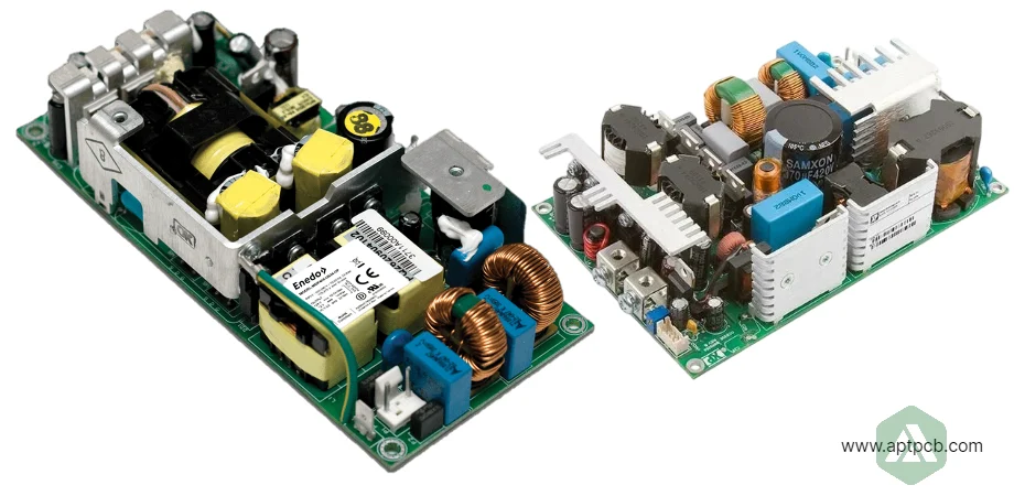
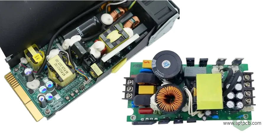
Switching mode power supply (SMPS) assemblies convert AC mains voltage to regulated DC outputs with 85-95% efficiency across computing, telecommunications, industrial automation, medical equipment, and consumer electronics requiring reliable operation through 50,000-100,000+ hours supporting critical infrastructure, life-safety systems, and everyday consumer products with comprehensive protection features, electromagnetic compatibility meeting international standards, and safety certifications enabling global market access.
At APTPCB, we deliver specialized switching power supply assembly services implementing flyback, forward, half-bridge, and resonant converter topologies across power ranges from 5W phone chargers through 3kW industrial supplies. Our turnkey assembly capabilities include component sourcing, PCB assembly, functional testing, and compliance validation supporting rapid product development and volume manufacturing.
Managing EMI and Conducted Emissions
Switching power supplies generate electromagnetic interference from high-speed switching (50-200kHz) requiring comprehensive filtering achieving compliance with conducted emissions limits (EN 55022 Class A/B, FCC Part 15 Class A/B) measuring 150kHz-30MHz on AC input lines. Inadequate filtering causes compliance test failures requiring expensive redesign, interference with adjacent equipment in installations, or field failures from EMI-induced control circuit malfunctions.
At APTPCB, our assembly services integrate validated EMI filtering ensuring first-pass compliance success.
Key EMI Management Techniques
Input Filter Implementation
- Common-mode (CM) choke using high-permeability ferrite cores with testing quality validated inductance values (typically 1-10mH per winding) attenuating high-frequency noise currents flowing through power and return lines
- Differential-mode (DM) inductors filtering asymmetric noise between line and neutral using powder core or gapped ferrite construction
- X-capacitors (typically 0.1-1μF film capacitors rated for line voltage) connecting line-to-neutral providing DM filtering while limiting inrush current during power-up
- Y-capacitors (typically 1-10nF ceramic capacitors rated >250VAC) connecting line/neutral to ground providing CM filtering while limiting leakage current below safety limits (typically <0.25mA for Class I, <0.1mA for Class II equipment)
- Multi-stage filtering using π or T configurations achieving >40dB attenuation at switching frequency and harmonics
- Component placement with functional testing validation maintaining filter integrity avoiding parasitic bypass paths degrading performance
PCB Layout Optimization
- Input filter grounding using single-point star grounding minimizing ground loop coupling between filter stages
- High-frequency capacitor placement close to noise sources providing local bypassing before propagation to input lines
- Trace routing minimizing loop areas between switching nodes and filter components reducing magnetic field coupling
- Ground plane segmentation separating noisy switching sections from sensitive control circuits using chassis ground as barrier
- Shielding integration when required using grounded copper barriers or metal shields over switching sections
- Layout validation through quality system design reviews ensuring EMI best practices followed
Component Selection and Characterization
- Common-mode choke selection balancing inductance, saturation current, and parasitic capacitance affecting high-frequency performance
- Film capacitor specification prioritizing low ESR and ESL maintaining filtering effectiveness at high frequencies
- Ferrite bead integration on control signals and auxiliary circuits preventing high-frequency coupling
- Proper component derating ensuring reliable operation despite voltage, current, and temperature stresses
- Supplier qualification validating component performance consistency across production lots
- Incoming quality control screening critical EMI components for specifications and counterfeit prevention
Radiated Emissions Control
- Switching frequency selection avoiding problematic bands when possible (e.g., AM broadcast 0.5-1.6MHz)
- Spread spectrum frequency modulation randomizing spectral content reducing peak amplitudes by 10-15dB
- Shielding enclosure design using properly gasketed metal enclosures with filtered I/O connections
- Cable management using shielded cables, ferrite beads, or proper twisted-pair routing minimizing antenna effects
- PCB-to-enclosure grounding using multiple low-impedance connections maintaining electromagnetic barrier integrity
- Pre-compliance testing during development using near-field probes and antennas identifying problem areas before formal testing
Compliance Testing and Validation
- Conducted emissions testing per CISPR 22 / EN 55022 using line impedance stabilization network (LISN) and calibrated receivers
- Radiated emissions testing in semi-anechoic chambers measuring field strength at 3m or 10m distances
- Immunity testing validating operation continues despite ESD, fast transients, surge, and RF interference
- International standards compliance supporting global markets including CE (Europe), FCC (US), CCC (China), VCCI (Japan)
- Test report generation and technical file preparation supporting regulatory submissions and customer audits
- Continuous compliance monitoring ensuring design changes or component substitutions maintain compliance
EMC Compliant Assembly
Through comprehensive EMI filtering, validated PCB layouts, and proven compliance testing procedures coordinated through our quality management systems, APTPCB delivers switching power supply assemblies achieving first-pass regulatory compliance supporting rapid market introduction and global sales.
Implementing Safety Isolation and Protection
Safety standards (UL 60950, IEC 62368, IEC 61010, UL 2601 medical) mandate reinforced or double isolation between AC mains and user-accessible outputs preventing electric shock hazards despite single-fault conditions. Implementation requires adequate creepage and clearance distances on PCBs, proper transformer construction, protective earth grounding, and comprehensive protection circuits detecting fault conditions triggering safe shutdown preventing fire, shock, or equipment damage hazards.
APTPCB implements validated safety features ensuring compliance with international safety standards.
Key Safety Implementation Requirements
Isolation Barrier Design
- Creepage distance (surface path between conductors) meeting standards based on working voltage, pollution degree, and material group (typically 6-8mm for reinforced isolation at 250VAC)
- Clearance distance (air gap between conductors) preventing arc-over during transient overvoltages (typically 4-6mm for reinforced isolation)
- PCB material selection using CTI (comparative tracking index) ≥175 for pollution degree 2 environments preventing carbon tracking under contamination
- Isolation slot routing cutting PCB material between primary and secondary eliminating potential conductive paths
- Layer assignment in multilayer PCBs maintaining isolation through core material with adequate dielectric strength
- NPI assembly prototyping validating isolation design before production commitment
Transformer Safety Construction
- Wire insulation using triple-insulated wire, separate bobbin sections, or insulation tape layers achieving required dielectric strength
- Primary-to-secondary spacing maintaining adequate distance preventing insulation breakdown
- Core-to-winding insulation using bobbin barriers or insulation sheets
- Winding arrangement minimizing interwinding capacitance reducing common-mode noise while maintaining safety
- Hipot testing applying 2x working voltage + 1000V for 60 seconds validating dielectric strength
- Partial discharge testing detecting corona or incipient insulation breakdown in high-voltage transformers
Protection Circuit Integration
- Input overvoltage protection using varistors (MOVs) clamping transients from lightning or switching events
- Input fuse selection coordinating with upstream circuit breakers and downstream component ratings
- Output overvoltage protection (OVP) using crowbar SCRs or control circuit shutdown preventing output exceeding safe limits
- Overcurrent protection (OCP) using current sensing and foldback limiting preventing thermal damage during overload
- Short circuit protection (SCP) immediately limiting current or shutting down during output shorts
- Overtemperature protection (OTP) monitoring heat sink or component temperatures triggering shutdown before thermal damage
Protective Earth and Grounding
- Class I equipment using protective earth connection bonding exposed metal parts to ground
- Y-capacitor grounding connecting EMI filter to protective earth or chassis providing noise path while limiting leakage current
- Fault current path design ensuring adequate conductor sizing and connections handling fault currents
- Ground loop prevention using proper star grounding topology avoiding circulating currents
- Touch current measurement validating leakage current remains within safety limits under normal and fault conditions
- Mass production testing including continuity checks verifying protective earth connections on every unit
Integrating Power Factor Correction
Power factor correction (PFC) circuits shape input current waveforms achieving power factor >0.9 and total harmonic distortion (THD) <10% meeting EN 61000-3-2 harmonic current limits mandatory for equipment >75W in European markets and increasingly adopted globally. PFC implementation improves grid power quality, enables higher power loading on circuits, and often improves efficiency and holdup time providing design benefits beyond regulatory compliance.
APTPCB assembles power supplies with integrated PFC stages meeting global efficiency and harmonic standards.
Key PFC Implementation
Active PFC Topology
- Boost PFC converter operating in continuous or critical conduction mode regulating DC bus voltage (typically 380-400VDC) while shaping input current
- Control IC implementation (Texas Instruments UCC28070, ON Semi NCP1654) providing average current mode control achieving PF >0.95
- Interleaved PFC using multiple phases reducing input current ripple and EMI while distributing thermal loads
- Digital PFC control enabling adaptive operation, diagnostics, and efficiency optimization across load ranges
- Inrush current limiting using NTC thermistors, active circuits, or relay bypass preventing excessive surge current during startup
- Component sourcing managing PFC MOSFETs, diodes, and inductors requiring high-voltage ratings and thermal capability
PFC Inductor Design
- Inductance value selection (typically 200-600μH) balancing ripple current, efficiency, and physical size
- Core material and geometry optimizing losses at 50-150kHz switching frequency
- Winding design minimizing AC resistance using Litz wire or multiple parallel strands
- Saturation current rating exceeding peak input current preventing core saturation and inductance collapse
- Thermal management through potting or heat sink integration maintaining core temperature <100°C
- Manufacturing qualification including inductance measurement, saturation testing, and thermal validation
Bulk Capacitor Selection
- Energy storage capacity providing holdup time (typically 10-20ms) during brief AC interruptions
- Voltage rating (typically 450V) withstanding elevated DC bus voltage with adequate margin
- Ripple current rating handling 120Hz rectified AC current and high-frequency switching ripple
- Temperature rating (105°C or 125°C) surviving elevated ambient and internal heating
- Lifetime estimation considering voltage, temperature, and ripple current stresses
- Capacitor monitoring and end-of-life detection enabling predictive maintenance in critical applications
Executing Comprehensive Production Testing
Switching power supply validation requires testing output regulation, efficiency, transient response, protection circuits, and safety features across input voltage ranges, output loads, and environmental conditions. Comprehensive testing prevents field failures from marginal designs, component variations, or manufacturing defects while enabling production throughput meeting cost targets through optimized test strategies and automation.
APTPCB provides dedicated power supply test capabilities validating all critical parameters.
Key Testing Requirements
Electrical Performance Testing
- Output voltage regulation measurement across line and load conditions verifying ±1-5% specifications
- Output ripple and noise measurement using oscilloscope and true-RMS meter quantifying AC content
- Efficiency measurement at multiple load points (25%, 50%, 75%, 100%) validating efficiency specifications and Energy Star compliance
- Transient response testing applying step load changes measuring voltage deviation and recovery time
- Cross-regulation testing on multi-output supplies verifying output voltage independence
- Holdup time measurement determining duration supply maintains regulation during input interruption
Protection Circuit Validation
- Overvoltage protection testing confirming OVP triggers at specified threshold preventing output exceeding safe limits
- Overcurrent and short circuit testing verifying current limiting and shutdown protect supply and load
- Overtemperature protection validation confirming thermal sensors trigger shutdown at specified temperatures
- Input overvoltage testing validating MOV and protection circuits withstand transients without damage
- Hiccup mode or auto-restart testing confirming proper recovery behavior after fault removal
- PCB conformal coating protection enabling reliable operation in humid or contaminated environments
Safety and Compliance Testing
- Hipot testing applying specified voltage between primary and secondary validating isolation integrity
- Leakage current measurement verifying touch current remains within safety limits
- Ground continuity testing confirming protective earth resistance meets specifications (<0.1Ω)
- Temperature rise testing measuring component temperatures under rated load conditions
- Conducted and radiated emissions pre-testing screening for compliance before formal certification
- Burn-in testing operating supplies at elevated temperature and stress identifying early failures
Environmental and Reliability Testing
- Temperature testing validating operation across specified ambient range (-40°C to +85°C for industrial)
- Humidity testing confirming reliable operation and storage in high-humidity environments
- Vibration and mechanical shock testing validating component attachment and structural integrity
- Power cycling accelerated life testing simulating years of on-off operation
- Thermal cycling between temperature extremes validating solder joint integrity and material compatibility
- MTBF prediction using component stress analysis estimating field reliability
Validated Production Quality
Through comprehensive test protocols, validated test equipment, and statistical process monitoring supported by our quality management systems, APTPCB delivers switching power supplies meeting electrical specifications, safety requirements, and reliability targets supporting successful product deployment.
Optimizing for Diverse Market Requirements
Switching power supplies serve diverse markets including consumer electronics (laptops, displays, appliances), telecommunications (base stations, network equipment), industrial (automation, motor drives), medical (patient monitoring, diagnostic equipment), and LED lighting (drivers, retrofit systems) requiring market-specific optimizations in efficiency standards, safety certifications, environmental ratings, and feature sets.
APTPCB provides flexible assembly supporting diverse market requirements through configurable platforms and comprehensive engineering support.
Key Market Optimization
Consumer Electronics
- Compact form factors and light weight maximizing product design flexibility
- Energy efficiency standards (DOE Level VI, ErP, Energy Star) minimizing standby power <0.1-0.3W
- Universal input (85-265VAC 47-63Hz) supporting global markets without modification
- Fast charging protocols (USB-PD, Quick Charge) delivering optimal power to mobile devices
- Cost optimization achieving consumer pricing targets through volume manufacturing
- Safety certifications (UL, CE, CCC, PSE, KC) enabling worldwide market access
Industrial and Automation
- Rugged construction withstanding harsh factory environments with dust, humidity, vibration
- Wide operating temperature range (-40°C to +70°C or +85°C) surviving unconditioned spaces
- DIN rail or chassis mounting accommodating standard industrial enclosures
- Industrial communication interfaces (Modbus, Profinet) enabling remote monitoring
- Mean time between failures >100,000 hours supporting minimal maintenance expectations
- Special certifications (UL508, UL61010) for industrial control equipment and test/measurement applications
Medical Equipment
- Medical safety standards compliance (IEC 60601, UL 2601) including patient leakage current limits
- Reinforced or double isolation preventing patient contact with hazardous voltages
- Low EMI emissions avoiding interference with sensitive medical instruments
- Reliability and uptime requirements supporting life-critical applications
- Quiet operation minimizing acoustic noise in patient care areas
- Auxiliary outputs providing standby power, communication, or indication signals
Telecommunications Infrastructure
- High reliability (>99.999% uptime) through redundant configurations and robust design
- 48V nominal input (36-75V operating range) matching telecom industry standards
- Operating temperature range (-40°C to +65°C or +75°C) surviving outdoor installations
- EMI compliance ensuring coexistence with sensitive communications equipment
- Network management (SNMP, PMBus) integrating into infrastructure monitoring systems
- 15-20 year service life matching telecommunications equipment expectations
Application-Optimized Manufacturing
By understanding diverse market requirements, implementing flexible manufacturing platforms, and providing comprehensive engineering support, APTPCB enables power supply manufacturers deploying optimized solutions across consumer, industrial, medical, and telecommunications markets worldwide.
Supporting Scalable Production and Cost Targets
Power supply manufacturing must balance quality, reliability, and cost meeting market pricing expectations while ensuring products survive specified operational lifetimes. Successful cost optimization requires design for manufacturing collaboration, process efficiency improvement, supply chain management, and continuous improvement programs reducing costs without compromising performance or reliability.
APTPCB delivers cost-effective power supply manufacturing through optimized processes and strategic partnerships.
Key Cost Optimization Strategies
Design for Manufacturing Collaboration
- Early DFM review identifying cost reduction opportunities through component standardization
- PCB optimization reducing layer count, panelization efficiency, and material costs
- Assembly process optimization minimizing difficult placements or special handling requirements
- Test strategy development balancing coverage against test time and equipment costs
- Component selection prioritizing availability, pricing stability, and second-source options
- Alternative component qualification providing flexibility during shortages or price increases
Process Efficiency and Automation
- High-speed automated assembly equipment maximizing throughput while maintaining quality
- Inline inspection (AOI, SPI) catching defects early preventing downstream rework
- Automated testing reducing labor costs while improving consistency and coverage
- Process optimization eliminating non-value-added steps and reducing cycle time
- Statistical process control enabling proactive quality management preventing defects
- Continuous improvement culture identifying and implementing efficiency gains
Supply Chain Management
- Strategic component sourcing leveraging volume commitments achieving competitive pricing
- Long-term supplier partnerships ensuring availability and pricing stability
- Component lifecycle monitoring proactively addressing obsolescence before availability issues
- Inventory optimization balancing carrying costs against production flexibility
- Logistics optimization consolidating shipments and optimizing packaging reducing costs
- Counterfeit prevention through authorized distributor relationships and incoming inspection
Volume Manufacturing Capability
- Scalable production capacity accommodating demand fluctuations from hundreds to millions annually
- Flexible manufacturing cells supporting product mix variations without extensive changeover
- Multi-site production capability providing redundancy and geographic optimization
- Quick response capability supporting rapid volume ramps during product launches
- Consistent quality across volume ranges maintaining reliability despite production scale
- Competitive pricing reflecting economies of scale while maintaining sustainable margins
Cost-Effective Volume Production
Through comprehensive cost optimization, efficient manufacturing processes, and strategic supply chain management, APTPCB enables power supply manufacturers achieving market-competitive pricing while maintaining quality and reliability requirements supporting successful products across diverse markets worldwide.